
- Forums
- Product Forums
- General Purpose MicrocontrollersGeneral Purpose Microcontrollers
- i.MX Forumsi.MX Forums
- QorIQ Processing PlatformsQorIQ Processing Platforms
- Identification and SecurityIdentification and Security
- Power ManagementPower Management
- Wireless ConnectivityWireless Connectivity
- RFID / NFCRFID / NFC
- Advanced AnalogAdvanced Analog
- Neural Processing UnitsNeural Processing Units
- MCX Microcontrollers
- S32G
- S32K
- S32V
- MPC5xxx
- Other NXP Products
- S12 / MagniV Microcontrollers
- Powertrain and Electrification Analog Drivers
- Sensors
- Vybrid Processors
- Digital Signal Controllers
- 8-bit Microcontrollers
- ColdFire/68K Microcontrollers and Processors
- PowerQUICC Processors
- OSBDM and TBDML
- S32M
- S32Z/E
-
- Solution Forums
- Software Forums
- MCUXpresso Software and ToolsMCUXpresso Software and Tools
- CodeWarriorCodeWarrior
- MQX Software SolutionsMQX Software Solutions
- Model-Based Design Toolbox (MBDT)Model-Based Design Toolbox (MBDT)
- FreeMASTER
- eIQ Machine Learning Software
- Embedded Software and Tools Clinic
- S32 SDK
- S32 Design Studio
- GUI Guider
- Zephyr Project
- Voice Technology
- Application Software Packs
- Secure Provisioning SDK (SPSDK)
- Processor Expert Software
- Generative AI & LLMs
-
- Topics
- Mobile Robotics - Drones and RoversMobile Robotics - Drones and Rovers
- NXP Training ContentNXP Training Content
- University ProgramsUniversity Programs
- Rapid IoT
- NXP Designs
- SafeAssure-Community
- OSS Security & Maintenance
- Using Our Community
-
- Cloud Lab Forums
-
- Knowledge Bases
- ARM Microcontrollers
- i.MX Processors
- Identification and Security
- Model-Based Design Toolbox (MBDT)
- QorIQ Processing Platforms
- S32 Automotive Processing Platform
- Wireless Connectivity
- CodeWarrior
- MCUXpresso Suite of Software and Tools
- MQX Software Solutions
- RFID / NFC
- Advanced Analog
- Neural Processing Units
-
- NXP Tech Blogs
- Home
- :
- QorIQプロセッシングプラットフォーム
- :
- QorIQ
- :
- Re: T2081 DDR3L Interface
T2081 DDR3L Interface
- RSS フィードを購読する
- トピックを新着としてマーク
- トピックを既読としてマーク
- このトピックを現在のユーザーにフロートします
- ブックマーク
- 購読
- ミュート
- 印刷用ページ
T2081 DDR3L Interface

- 新着としてマーク
- ブックマーク
- 購読
- ミュート
- RSS フィードを購読する
- ハイライト
- 印刷
- 不適切なコンテンツを報告
Hi,
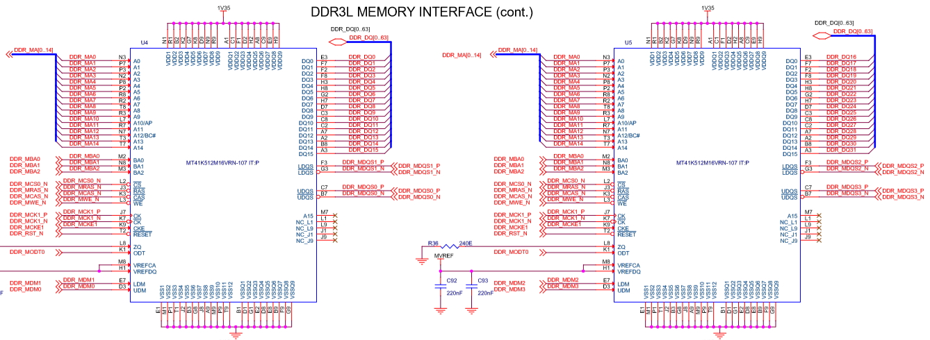
Currently I am working on the design which involve DDR3 (MT41K512M16VRN-107 IT:P) interface with T2081. I am attaching the screenshot of my interface for your reference.
I have the following queries:
1) As in T2081, we have 4 chip select line, how do I identified how many CS lines I required in my design? (Currently I am using only one CS line in my design).
2) We have two clock line (mck0, ~mck0 and mck1, ~mck1) in t2081, is it necessary to use both the diff. clock in the design? (I am using both the clock in my design)
3) Importance of MODT0 and MODT1? Can I use both or just one line is enough? (Currently I am using only one in my design)
4) In DDR IC (MT41K512M16VRN-107 IT:P), we have LDM and UDM pin? can I reverse the connection in those pins? Does reversing the connection will cause the performance issue? (Please check the attached image)
Waiting to hear from you soon.
T2081: Layout DDR3 and other High Speed Signals
Regards
Hemant
 ufedor
- 新着としてマーク
- ブックマーク
- 購読
- ミュート
- RSS フィードを購読する
- ハイライト
- 印刷
- 不適切なコンテンツを報告
1) Chip-select corresponds to memory bank. For one memory bank one chip-select has to be used.
2) Please refer to the AN3940 - Hardware and Layout Design Considerations for DDR3 SDRAM, Table 1. DDR3 designer checklist, 46:
"Ensure one clock pair is used for each chip-select. The clock pair should follow the address/command/control signal groups in fly-by topology."
3) The processor has four MODT[0: 3] signals. Each MODTn signal corresponds to specific chip-select - refer to the AN3940, Table 1. DDR3 designer checklist, 37:
" Connect each of the MODT signals that are in the same group to the same physical memory bank:
- MODT(0), MCS(0), MCKE(0)
- MODT(1), MCS(1), MCKE(1)
- MODT(2), MCS(2), MCKE(2)
- MODT(3), MCS(3), MCKE(3)"
4) You wrote:
> ? can I reverse the connection in those pins?
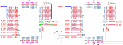
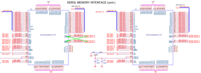
In the provided pictures connections are incorrect.
Please consider that DQS belongs to specific byte lane as specified in the AN3940, Table 1. DDR3 designer checklist, 25:
""Route all signals within a given byte lane on the same critical layer with the same via count. Assuming ECC
is used, the DDR3 data bus consists of nine data byte lanes.
Note: The byte ordering below is not a requirement; byte lanes can be routed in the order that best fits the
user’s application.
- Byte lane 0—MDQ(7:0), MDM(0), MDQS(0), MDQS(0)
- Byte lane 1—MDQ(15:8), MDM(1), MDQS(1), MDQS(1)
- Byte lane 2—MDQ(23:16), MDM(2), MDQS(2), MDQS(2)
- Byte lane 3—MDQ(31:24), MDM(3), MDQS(3), MDQS(3)
- Byte lane 4—MDQ(39:32), MDM(4), MDQS(4), MDQS(4)
- Byte lane 5—MDQ(47:40), MDM(5), MDQS(5), MDQS(5)
- Byte lane 6—MDQ(55:48), MDM(6), MDQS(6), MDQS(6)
- Byte lane 7—MDQ(63:56), MDM(7), MDQS(7), MDQS(7)
- Byte lane 8—MECC(7:0), MDM(8), MDQS(8), MDQS(8)"
- 新着としてマーク
- ブックマーク
- 購読
- ミュート
- RSS フィードを購読する
- ハイライト
- 印刷
- 不適切なコンテンツを報告
ufedor
- 新着としてマーク
- ブックマーク
- 購読
- ミュート
- RSS フィードを購読する
- ハイライト
- 印刷
- 不適切なコンテンツを報告
Please read the response 4) and see corrections in the pictures.


- 新着としてマーク
- ブックマーク
- 購読
- ミュート
- RSS フィードを購読する
- ハイライト
- 印刷
- 不適切なコンテンツを報告
THANKYOU FOR YOUR REPLY. I WILL DO THE CHANGES.
1)Also in the design, instead of using MCK0 AND MCK1, CAN I USE ONLY SINGLE MCK0 FOR ALL THE DDR INCLUDING ECC?
2)Can i use only one chip select for all my DDR IC shown in the picture? if yes, please explain.
3)In t2081, we have only two on die termination? Again can i use only one for all the DDR IC? if yes, please explain
Regards
Hemant
ufedor
- 新着としてマーク
- ブックマーク
- 購読
- ミュート
- RSS フィードを購読する
- ハイライト
- 印刷
- 不適切なコンテンツを報告
Please thoroughly read previous answers and the AN3940 before asking further questions.
