- NXP Forums
- Product Forums
- General Purpose MicrocontrollersGeneral Purpose Microcontrollers
- i.MX Forumsi.MX Forums
- QorIQ Processing PlatformsQorIQ Processing Platforms
- Identification and SecurityIdentification and Security
- Power ManagementPower Management
- MCX Microcontrollers
- S32G
- S32K
- S32V
- MPC5xxx
- Other NXP Products
- Wireless Connectivity
- S12 / MagniV Microcontrollers
- Powertrain and Electrification Analog Drivers
- Sensors
- Vybrid Processors
- Digital Signal Controllers
- 8-bit Microcontrollers
- ColdFire/68K Microcontrollers and Processors
- PowerQUICC Processors
- OSBDM and TBDML
-
- Solution Forums
- Software Forums
- MCUXpresso Software and ToolsMCUXpresso Software and Tools
- CodeWarriorCodeWarrior
- MQX Software SolutionsMQX Software Solutions
- Model-Based Design Toolbox (MBDT)Model-Based Design Toolbox (MBDT)
- FreeMASTER
- eIQ Machine Learning Software
- Embedded Software and Tools Clinic
- S32 SDK
- S32 Design Studio
- Vigiles
- GUI Guider
- Zephyr Project
- Voice Technology
- Application Software Packs
- Secure Provisioning SDK (SPSDK)
- Processor Expert Software
-
- Topics
- Mobile Robotics - Drones and RoversMobile Robotics - Drones and Rovers
- NXP Training ContentNXP Training Content
- University ProgramsUniversity Programs
- Rapid IoT
- NXP Designs
- SafeAssure-Community
- OSS Security & Maintenance
- Using Our Community
-
-
- Home
- :
- QorIQ Processing Platforms
- :
- QorIQ
- :
- Re: LS1046A : Discrete DDR4 General Questions
LS1046A : Discrete DDR4 General Questions
- Subscribe to RSS Feed
- Mark Topic as New
- Mark Topic as Read
- Float this Topic for Current User
- Bookmark
- Subscribe
- Mute
- Printer Friendly Page
LS1046A : Discrete DDR4 General Questions
- Mark as New
- Bookmark
- Subscribe
- Mute
- Subscribe to RSS Feed
- Permalink
- Report Inappropriate Content
Hello,
I develop a custom board with the LS1046A CPU.
We would like to use 2GB of DDR4 memory +ECC for our custom board.
I have connected 3x DDR4 MT40A512M16TB-062E:J memory (1GB, 512*16) from Micron on the LS1046A CPU DDR memory interface.
My questions:
1) Is it ok to use only D1_MCS0_B, D1_ODT0, D1_MCKE0 and D1_MBG0 signals with D1_MCK0 clock for the 3 DDR memory as the LS1046 Freeway board ?
2) In the schematic of the LS1046 Freeway board, on the ECC DDR4, unused DQ line are left unconnected
Whereas, in the Hardware and Layout Design Considerations for DDR4 SDRAM Memory Interfaces, it is wrote :
"When 16-bit DRAM is used for ECC byte lane, ensure the eight unused DQ pins are pulled up. Strobes DQS,nDQS and DM inputs should be tied via resistor to their nonactive power levels (GND or VDD)."
What is the best way to do?
3) According to Hardware and Layout Design Considerations for DDR4 SDRAM Memory Interfaces :
"If multiple physical banks are needed, double stack (top and bottom) the banks to prevent lengthy and undesirable address/cmd topologies."
Is one physical banks => one DDR4 chip?
What is double stack? Is it one DDR4 on top and one on bottom of the PCB at the same coordonate x-y?
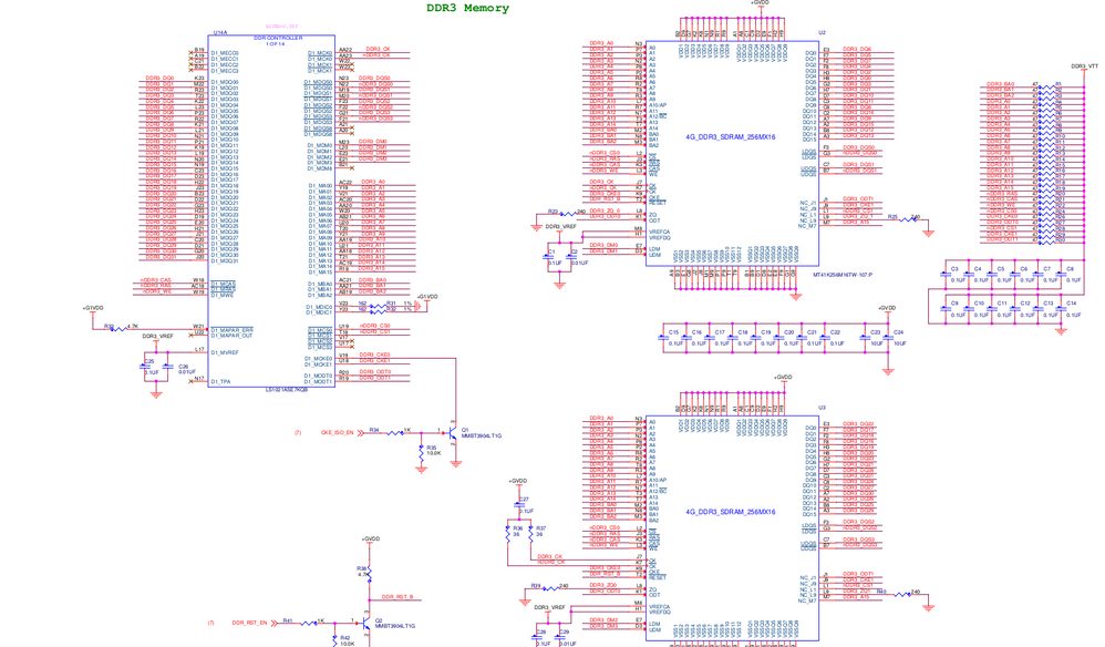
4) I see on the LS1046A Freeway baord schematic that DDR_VTT has its decoupling capacitors with GVDD with no bulk capacitor. Why is these capacitors are not connected between DDR_VTT and GND? What is the best way to do? None of the documentation I have found talk about this kind of decoupling.
Why no bulk capacitor (47-220uF) as mention in Hardware and Layout Design Considerations for DDR4 SDRAM Memory Interfaces?
Thank you
- Mark as New
- Bookmark
- Subscribe
- Mute
- Subscribe to RSS Feed
- Permalink
- Report Inappropriate Content
I noticed that the reference board using 4*16bit DDR4 or 2*16bit DDR4 for memory interface for 32bit data, can we use 1*32bit DDR4 ?, is there any advantage using multiple DDR4 with lower data width ?
- Mark as New
- Bookmark
- Subscribe
- Mute
- Subscribe to RSS Feed
- Permalink
- Report Inappropriate Content
I believe that PCB layout of the 2x16 can be plainer than 1x32.
- Mark as New
- Bookmark
- Subscribe
- Mute
- Subscribe to RSS Feed
- Permalink
- Report Inappropriate Content
1) Actually it is a must - refer to the AN5097 - Hardware and Layout Design Considerations for DDR4 SDRAM, Table 1. DDR4 design checklist, 50:
"Ensure one clock pair is used for each chip-select. The clock pair should follow the address/command/control signal groups in fly-by topology."
2) The AN recommendation is reasonable.
3) You wrote:
> Is one physical banks => one DDR4 chip?
In your case one bank consists of three SDRAM devices.
> What is double stack?
> Is it one DDR4 on top and one on bottom of the PCB at the same coordonate x-y?
Correct.
4) The AN contains "universal" recommendation.
In case of the FRWY board it was tested that DDR_VTT is stable enough with C1533 and C1534.
- Mark as New
- Bookmark
- Subscribe
- Mute
- Subscribe to RSS Feed
- Permalink
- Report Inappropriate Content
Thank you for your quick responses!
One question was not responded, 3) Why are these capacitors not connected between DDR_VTT and GND? What is the best way to do?
Why do you connect your decoupling capacitors between DDR_VTT and GVDD? Why not GND?
Thank you
- Mark as New
- Bookmark
- Subscribe
- Mute
- Subscribe to RSS Feed
- Permalink
- Report Inappropriate Content
VTT is middle voltage level between GVDD and GND, Putting decoupling capacitors between VTT and GVDD has the same effect with putting them between VTT and GND,
