
- Forums
- Product Forums
- General Purpose MicrocontrollersGeneral Purpose Microcontrollers
- i.MX Forumsi.MX Forums
- QorIQ Processing PlatformsQorIQ Processing Platforms
- Identification and SecurityIdentification and Security
- Power ManagementPower Management
- Wireless ConnectivityWireless Connectivity
- RFID / NFCRFID / NFC
- Advanced AnalogAdvanced Analog
- Neural Processing UnitsNeural Processing Units
- MCX Microcontrollers
- S32G
- S32K
- S32V
- MPC5xxx
- Other NXP Products
- S12 / MagniV Microcontrollers
- Powertrain and Electrification Analog Drivers
- Sensors
- Vybrid Processors
- Digital Signal Controllers
- 8-bit Microcontrollers
- ColdFire/68K Microcontrollers and Processors
- PowerQUICC Processors
- OSBDM and TBDML
- S32M
- S32Z/E
-
- Solution Forums
- Software Forums
- MCUXpresso Software and ToolsMCUXpresso Software and Tools
- CodeWarriorCodeWarrior
- MQX Software SolutionsMQX Software Solutions
- Model-Based Design Toolbox (MBDT)Model-Based Design Toolbox (MBDT)
- FreeMASTER
- eIQ Machine Learning Software
- Embedded Software and Tools Clinic
- S32 SDK
- S32 Design Studio
- GUI Guider
- Zephyr Project
- Voice Technology
- Application Software Packs
- Secure Provisioning SDK (SPSDK)
- Processor Expert Software
- Generative AI & LLMs
-
- Topics
- Mobile Robotics - Drones and RoversMobile Robotics - Drones and Rovers
- NXP Training ContentNXP Training Content
- University ProgramsUniversity Programs
- Rapid IoT
- NXP Designs
- SafeAssure-Community
- OSS Security & Maintenance
- Using Our Community
-
- Cloud Lab Forums
-
- Knowledge Bases
- ARM Microcontrollers
- i.MX Processors
- Identification and Security
- Model-Based Design Toolbox (MBDT)
- QorIQ Processing Platforms
- S32 Automotive Processing Platform
- Wireless Connectivity
- CodeWarrior
- MCUXpresso Suite of Software and Tools
- MQX Software Solutions
- RFID / NFC
- Advanced Analog
- Neural Processing Units
-
- NXP Tech Blogs
- RSS フィードを購読する
- トピックを新着としてマーク
- トピックを既読としてマーク
- このトピックを現在のユーザーにフロートします
- ブックマーク
- 購読
- ミュート
- 印刷用ページ
SGTL5000 Lineout Problem
- 新着としてマーク
- ブックマーク
- 購読
- ミュート
- RSS フィードを購読する
- ハイライト
- 印刷
- 不適切なコンテンツを報告
Dears,
I used SGTL5000+i.MX6 to debug voice lineout. The first time to trigger voice line out may lead to voice very low, then if trigger in less than 5 seconds, the voice line out may work normal. If trigger more than 5 seconds, the same problem may reappear.
Can you please kindly help to advice?
BRs,
Ray
- 新着としてマーク
- ブックマーク
- 購読
- ミュート
- RSS フィードを購読する
- ハイライト
- 印刷
- 不適切なコンテンツを報告
Hi,
Can you please share the SGTL5000 configuration? Pleas also confirm if you are using ALSA (Advanced Linux Sound Architecture).
Are you using an NXP evaluation board? We want to see if we can reproduce the issue with our boards and check if it could be a linux problem or an issue related to the i.MX, or confirm if it a problem with the SGTL5000 Codec.
For the kind of issue you are mentioning, I’m thinking this could be a problem caused by linux if there are too many pending tasks to run.
Regards,
Jose
- 新着としてマーク
- ブックマーク
- 購読
- ミュート
- RSS フィードを購読する
- ハイライト
- 印刷
- 不適切なコンテンツを報告
Hi Reyes,
Thanks for your kindly help.
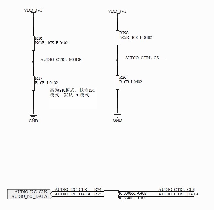
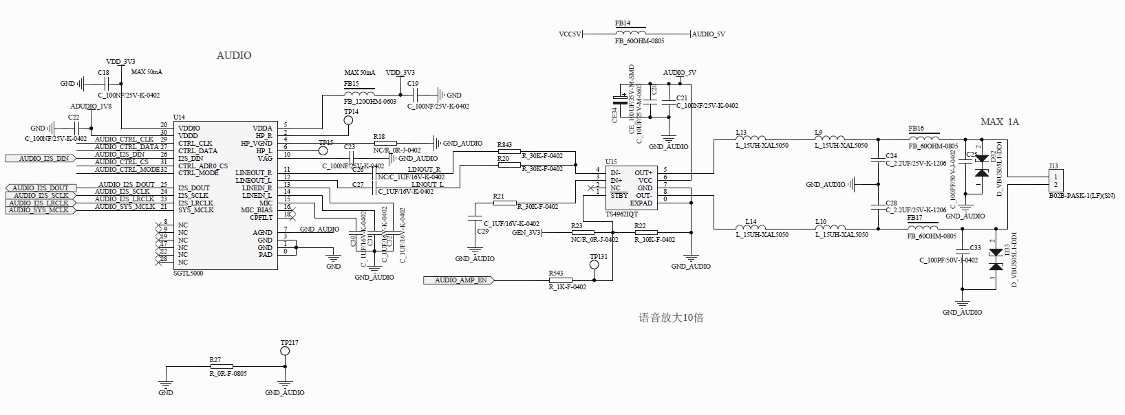
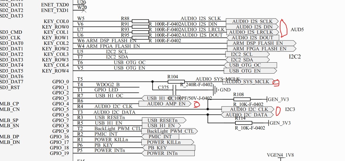
Please check schematics and SGTL5000 configuration attached.
Customer used ALSA, it just run at customer's board, not NXP EVK.
Also, no pending tasks.
Can you please kindly help to advice?
BRs,
Ray
- 新着としてマーク
- ブックマーク
- 購読
- ミュート
- RSS フィードを購読する
- ハイライト
- 印刷
- 不適切なコンテンツを報告
Hi Ray,
From the HW perspective, I don’t see any problem on the schematic. Just please confirm if the ADUDIO_1V8 voltage connected to VDDD pin of the codec is generated from the SGTL5000 device or if is generated by an external regulator. Because of the 100nF capacitor connected in this pin, I’m thinking the voltage is generated by an external regulator, which is correct.
I ask because of the issues with VDDD regulator and why is recommended for new designs to power it externally, you can find the document in the following link: https://www.nxp.com/docs/en/errata/SGTL5000ER.pdf
Now, regarding the SW configuration:
According to your SSS_CTRL->DAC_SELECT = 0x1 = I2S_IN configuration, you are bypassing DAP and connecting the I2S input directly to the DAC.
When I2S IN -> DAC -> LINEOUT route is selected, output Level (when VDDIO and VDDA are 3.3V) is 1.0 Vrms.
Power up the digital and Analog interfaces used (I2S_IN and DAC) using the following bits:
* CHIP_DIG_POWER 0x0002
To power up the I2S_IN (I2S_IN_POWERUP - Bit 0) and the DAC (DAC_POWERUP – bit 5)
* CHIP_ANA_POWER 0x0030
To power up the DAC use DAC_POWERUP
Some extra configuration is needed in the DAC to complete the setting:
The DAC output has a digital volume control from -90 dB to 0 dB in ~0.5 dB step sizes. The register CHIP_DAC_VOL controls the DAC volume.
The line output has a dedicated gain stage that can be used to adjust the output level. The CHIP_LINE_OUT_VOL controls the line level output gain.
The line outputs also have a dedicated mute that is controlled by the register field CHIP_ANA_CTRL- >MUTE_LO, you need to make sure it is not activated for your application.
You can find an example about how to initialize the SGTL5000 in the following link: https://www.nxp.com/docs/en/application-note/AN3663.pdf
Regards,
Reyes
- 新着としてマーク
- ブックマーク
- 購読
- ミュート
- RSS フィードを購読する
- ハイライト
- 印刷
- 不適切なコンテンツを報告
Thanks, Reyes,
We tested with customer, seems the POP voice cannot be avoid only after 400ms delay.
Do you have any advice?
BRs,
Ray
- 新着としてマーク
- ブックマーク
- 購読
- ミュート
- RSS フィードを購読する
- ハイライト
- 印刷
- 不適切なコンテンツを報告
Hi Ray,
I’m not sure if I understand, are you saying that you can hear the POP noise from the moment you turn-on the Codec, and after a 400ms this noise issue is eliminated?
My recommendation would be to set the “SMALL_POP” bit in CHIP_REF_CTRL 0x0028. Setting this bit slows down the VAG ramp from ~200 to ~400 ms to reduce the startup pop/thunk noise.
Take in mind that enabling this bit increases the turn on/off time.
Another recommendation to avoid any pops/clicks (spikes), would be to mute the outputs during the chip configuration steps.
Regards,
Reyes