- Forums
- Product Forums
- General Purpose MicrocontrollersGeneral Purpose Microcontrollers
- i.MX Forumsi.MX Forums
- QorIQ Processing PlatformsQorIQ Processing Platforms
- Identification and SecurityIdentification and Security
- Power ManagementPower Management
- Wireless ConnectivityWireless Connectivity
- RFID / NFCRFID / NFC
- Advanced AnalogAdvanced Analog
- MCX Microcontrollers
- S32G
- S32K
- S32V
- MPC5xxx
- Other NXP Products
- S12 / MagniV Microcontrollers
- Powertrain and Electrification Analog Drivers
- Sensors
- Vybrid Processors
- Digital Signal Controllers
- 8-bit Microcontrollers
- ColdFire/68K Microcontrollers and Processors
- PowerQUICC Processors
- OSBDM and TBDML
- S32M
- S32Z/E
-
- Solution Forums
- Software Forums
- MCUXpresso Software and ToolsMCUXpresso Software and Tools
- CodeWarriorCodeWarrior
- MQX Software SolutionsMQX Software Solutions
- Model-Based Design Toolbox (MBDT)Model-Based Design Toolbox (MBDT)
- FreeMASTER
- eIQ Machine Learning Software
- Embedded Software and Tools Clinic
- S32 SDK
- S32 Design Studio
- GUI Guider
- Zephyr Project
- Voice Technology
- Application Software Packs
- Secure Provisioning SDK (SPSDK)
- Processor Expert Software
- Generative AI & LLMs
-
- Topics
- Mobile Robotics - Drones and RoversMobile Robotics - Drones and Rovers
- NXP Training ContentNXP Training Content
- University ProgramsUniversity Programs
- Rapid IoT
- NXP Designs
- SafeAssure-Community
- OSS Security & Maintenance
- Using Our Community
-
- Cloud Lab Forums
-
- Knowledge Bases
- ARM Microcontrollers
- i.MX Processors
- Identification and Security
- Model-Based Design Toolbox (MBDT)
- QorIQ Processing Platforms
- S32 Automotive Processing Platform
- Wireless Connectivity
- CodeWarrior
- MCUXpresso Suite of Software and Tools
- MQX Software Solutions
- RFID / NFC
- Advanced Analog
-
- NXP Tech Blogs
- Home
- :
- Model-Based Design Toolbox (MBDT)
- :
- NXP Model-Based Design Tools Knowledge Base
- :
- UCANS32K1SIC EVB Application Development using Model-Based Design Toolbox
UCANS32K1SIC EVB Application Development using Model-Based Design Toolbox
- Subscribe to RSS Feed
- Mark as New
- Mark as Read
- Bookmark
- Subscribe
- Printer Friendly Page
- Report Inappropriate Content
UCANS32K1SIC EVB Application Development using Model-Based Design Toolbox
UCANS32K1SIC EVB Application Development using Model-Based Design Toolbox
1. Introduction
This article shows how to develop an application for the UCANS32K1SIC evaluation board in MATLAB® and Simulink® and NXP®’s Model-Based Design Toolbox.
1.1. General purpose
The UCANS32K1SIC is a CAN signal improvement capability (SIC) evaluation board designed for both automotive (ADAS, Body Control Units etc.) and industrial applications (Building Control, Servos, Mobile Robotic, etc.)
In total, there are three UCANS32K1 evaluation boards:
- UCANS32K146-01
- UCANS32K1SCT
- UCANS32K1SIC
In this article, we choose to focus only on one of them, the UCANS32K1SIC evaluation board.
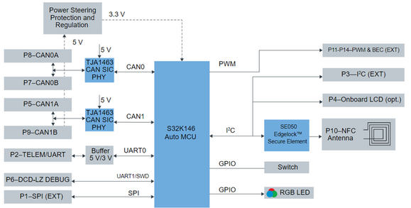
The UCANS32K1SIC provides two CAN SIC interfaces and is based on the S32K146 (32-bit Arm® Cortex®-M4) from the S32K microcontroller family. Also, the UCANS32K1SIC features EdgeLock® SE050 secure element for authentication and encryption development. For complete details, please access the following link
1.2. Block Diagram
2. The UCANS32K1SIC application example model
The UCANS32K1SIC application example proposed in this article (ucans32k1sic_mbd_4_3_0) implements the following actions:
- Controls the RGB LED (GPO)
- Reads the Switch state (GPI)
- Displays messages on the LCD screen (“Red Led On”, “Green Led On”, “Blue Led On”) using the I2C communication protocol
- Adds FreeMASTER communication via UART protocol
- Configures both instances of the CAN communication protocol (CAN0 and CAN1) and sends/receives messages
2.1. Prerequisite Software
For the development of this application, the following software is required:
- MATLAB® and Simulink® (minimum 2020a)
- Stateflow®
- MATLAB Coder™
- Simulink Coder™
- Embedded Coder® Support Package for ARM Cortex-M Processors
- Model-Based Design Toolbox for S32K1xx 4.3.0
- FreeMASTER Run-Time Debugging Tool 3.2
2.2. Prerequisite Hardware
For the development of this application, the following hardware is required:
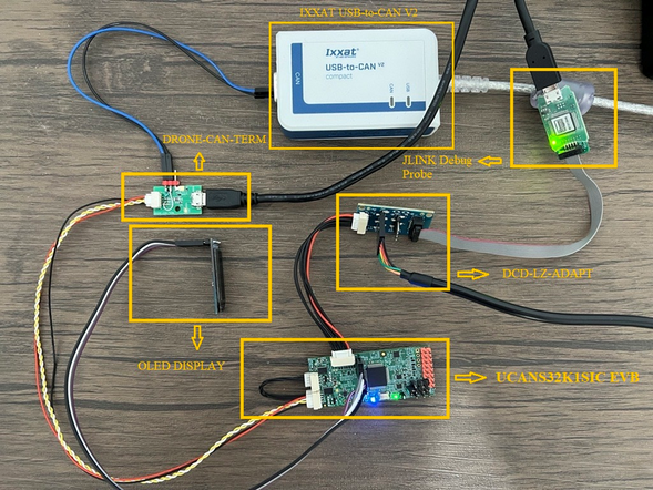
- UCANS32K1SIC evaluation board
- DCD-LZ-ADAPT debug adapter with cable, which provides breakout connectors for SWD/JTAG Debugger and FTDI USB-UART
- CAN Bus Terminator (DRONE-CAN-TERM) with MicroUSB cable
- CAN cable terminated on both ends
- OLED Display 128x64 pixels
- JLink Debug Probe (or any other compatible SWD probe)
- IXXAT USB-to-CAN V2 (or any other canAnalyser )
3. Simulink model implementation and blocks configuration
After the NXP Model-Based Design Toolbox for S32K1xx is installed, the next step is to open the library and drag and drop the necessary blocks.
The MCU configuration with MBD_S32K1xx_Config_Implementation block
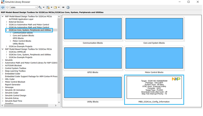
The first step is to add the MBD_S32K1xx_Config_Information into our Simulink model. This action makes the model aware that it will generate code for the S32K1 microcontroller.
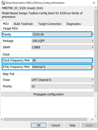
Once opening the block, the user needs to choose the processor family inside the MCU tab. For this particular board, the processor is S32K146.
Then the system clock frequency (MHz) must also be specified:
- Clock Frequency Value (80 MHz)
- External Crystal clock - 8 MHz (check the schematics or other materials)
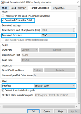
In the Target Connection tab, the following settings are required: The download interface JTAG and SEGGER JLink software. In our case, the kit comes with the SEGGER JLink so we are selecting this one. In case the JLink software is installed at a different location than the default one, the correct path shall be indicated in the “SEGGER JLink installation path” field.
3.1. Reads the Switch state (GPI)
In this application, each push of the button selects which color of the RGB LED is lighten up. So, to be able to control that, the state of the button needs to be read. A variable named “counter” stores the values corresponding to each state (0-RED, 1-GREEN, 2-BLUE).
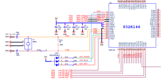
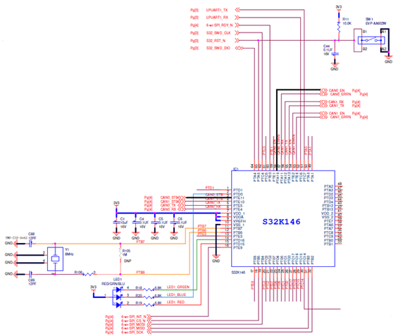
The pin corresponding to the SW button reading must be configured (using the schematic for the UCANS32K1SIC evaluation board).
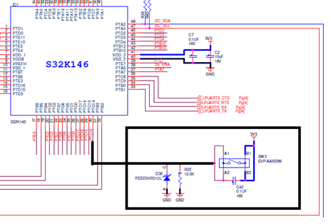
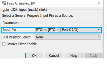
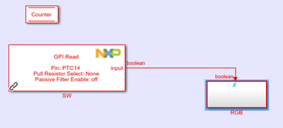
With each execution of the main step in the model, the GPI Read block triggers the subsystem where the states of the LED are changed.
3.2. Controls the RGB LED (GPO)
When the counter is incremented, the LED changes its state (RED-GREEN-BLUE).
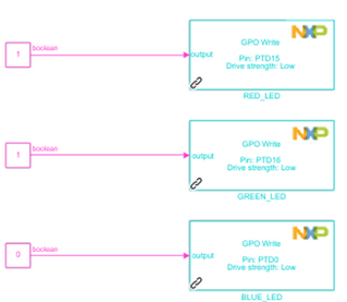
This is implemented using the GPO Write blocks.
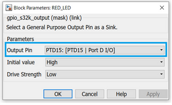
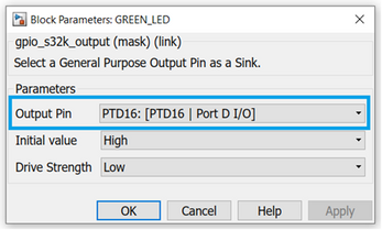
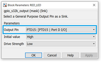
The pins corresponding to each LED color must be configured according to the schematic.
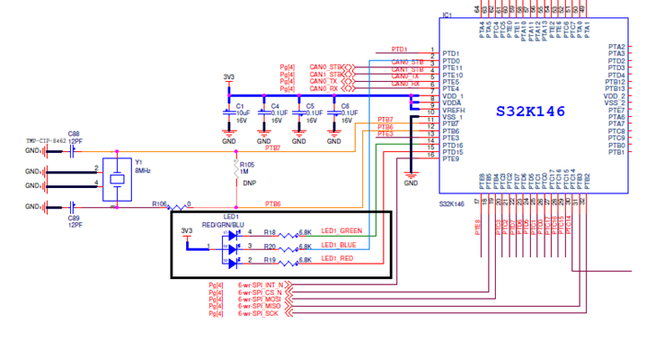
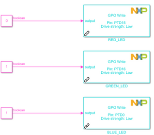
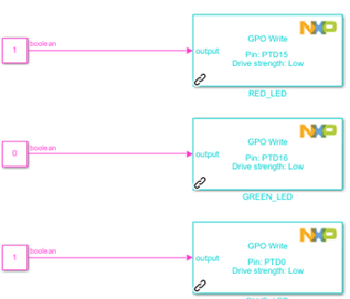
After identifying each pin, they must be set in GPO write blocks as follows:
To turn on one of the LEDs colors, set the pin to 0 and to turn it off set it to 1. This is because the LED anode is routed to 3V3 and the cathode is connected to the pin. When the application requires to turn on only one color, the others must be turned off, as might be seen in the screenshots below.
3.3. Displays messages on the LCD screen (“Red Led On”, Green Led On”, “Blue Led On”) using the I2C communication protocol
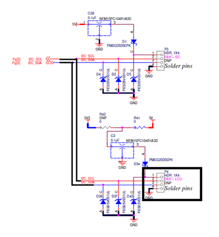
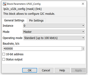
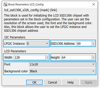
For this example, the OLED display used is 128 x 64 pixels. The LCD communicates with MCU via LPI2C0 (P4). So, in order to communicate with the OLED display, the LPI2C instance must be first configured.
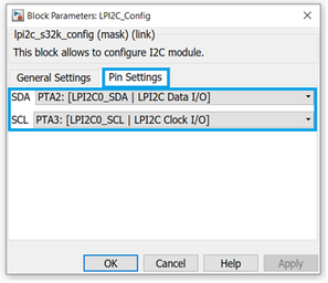
LPI2C0 block configuration:
The pins corresponding to LPI2C0 instance must be configured according to the schematic.

Next, the OLED block needs to be configured as follows:
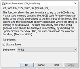
After the LPI2C0 and OLED blocks are configured, messages can be displayed on the LCD screen using the LCD Write String block.
LCD Write String block configuration:
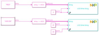
To display the other messages (GREEN LED ON and BLUE LED ON), the steps are the same.
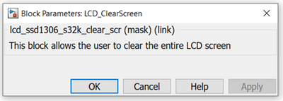
To clear the LCD screen and display another message, the LCD Clear Screen must be used.
3.4. FreeMASTER project via UART protocol
FreeMASTER is a user-friendly real-time debug monitor and data visualization tool that enables runtime configuration and tuning of embedded software applications.
The FreeMASTER block configuration from NXP MBDT for the S32K1xx library uses the following communication interfaces:
- UART
- CAN
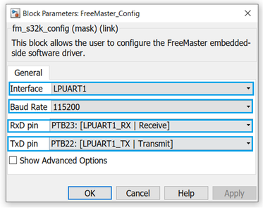
In this example, we used the LPUART1 interface to send/receive messages from the FreeMASTER application.
The pins corresponding to LPUART1 (they are routed to the P6 connector) instance must be configured according to the schematic.
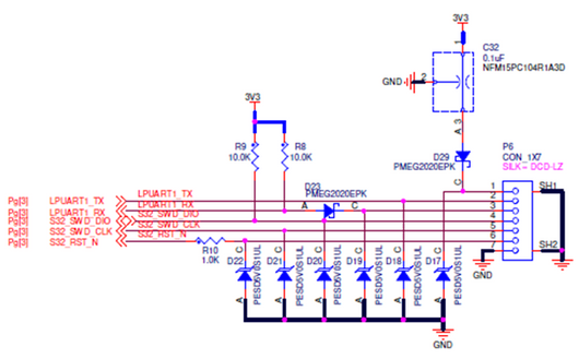
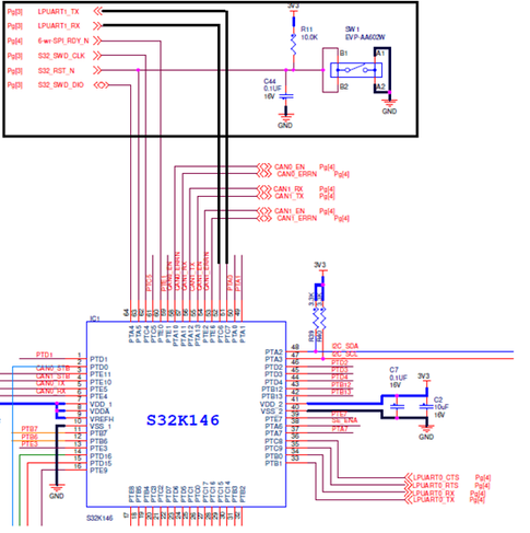
The RxD and TxD pins required routed in the schematics are PTC6 and PTC7. Another parameter that must be configured is the Baud Rate (maximum number of bits per second to be transferred). For this application, the Baud Rate is 115200 kbps.
3.5. Configures of both instances of the CAN communication protocol (CAN0 and CAN1) and sends/receives messages
In this subchapter, the goal is to show how to receive/send messages on both CAN instances (CAN0 and CAN1).
- CAN0 instance
First, CAN0 instance needs to be configured. For this action, the CAN configuration block is required.
In the General tab, the following settings are:
- Module: 0 (for the CAN0 instance)
- Operational Mode: Normal mode
- Max number of MBs (1-32): 16
- The RxD and TxD pins required are: PTE4 and PTE5 (according to the schematic)

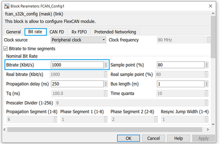
In the Bit rate tab, the default Bitrate is 1000Kbit/s, but it depends on the case.
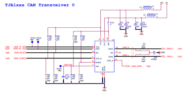
The next step is to choose the operating mode for the CAN transceiver (for UCANS32K1SIC, the CAN transceiver is TJA1463).
The TJA1463 is a member of the TJA146x family of transceivers that provide an interface between a Controller Area Network (CAN) or CAN FD (Flexible Data rate) protocol controller and the physical two-wire CAN bus.
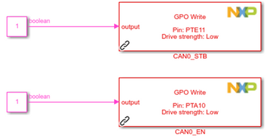
Control pins STB_N and EN are used to select the operating mode. To simplify the application, the Normal mode has been selected to be set for the entire execution of the application.
HIGH-level state on pin STB_N and pin EN selects Normal mode.
According to the schematic, for the instance of CAN0, the corresponding pins for STB_N and EN are PTE11 and PTA10.
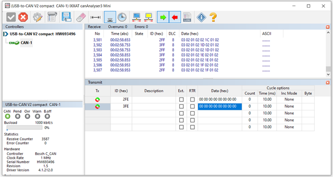
For checking the correctness of the configuration of the settings and application, the transceiver outputs CAN_H and CAN_L are connected to CAN Analyzer, while messages are sent from the PC.
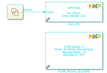
A numeric sequence with the ID 0x3FF is sent continuously while a message received with ID 0x3FE toggles the PTD15 (Red LED) on each receive.
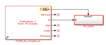
To receive a CAN message asynchronous with the application, the CAN receive interrupt must be used.
When a message is received, it triggers the subsystem Rx_0x3FE.
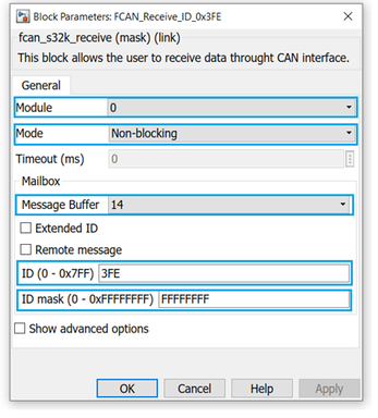
The fcan_s32l_receive block configuration is:
- Module: 0
- Mode: Non-blocking
- Message Buffer: 14
- ID: 3FF
- ID mask: FFFFFFFF
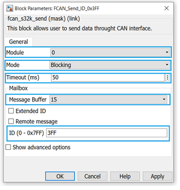
To send a message with the ID 0x3FF on CAN0, in the fcan_s32l_send block, the following settings are required:
- Module: 0
- Mode: Blocking
- Timeout (ms): 50
- Message Buffer: 15
- ID: 3FF
- CAN1 instance
For the instance of CAN1, the steps are the same as above (the configuration of CAN0), but this time a numeric sequence with ID 0x2FF is sent continuously and a received message with ID 0x3FF will toggle the PTD16 (Green LED) on each receive.
A CAN Analyzer is needed to analyze and collect data from the CAN bus and display them on the PC.
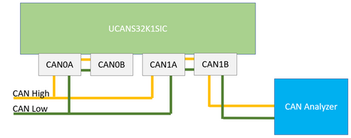
To use both CAN instances on the same CAN Analyzer, a hardware connection is needed between CAN0A and CAN1A (or any CAN0 with CAN1).
This can be seen in the following diagram:
In this application, the CAN Analyzer used is IXXAT USB-to-CAN V2 and the software interface is IXXAT canAnalyser3 Mini, but of course, any other CAN Analyzer can be used.
4. Model overview
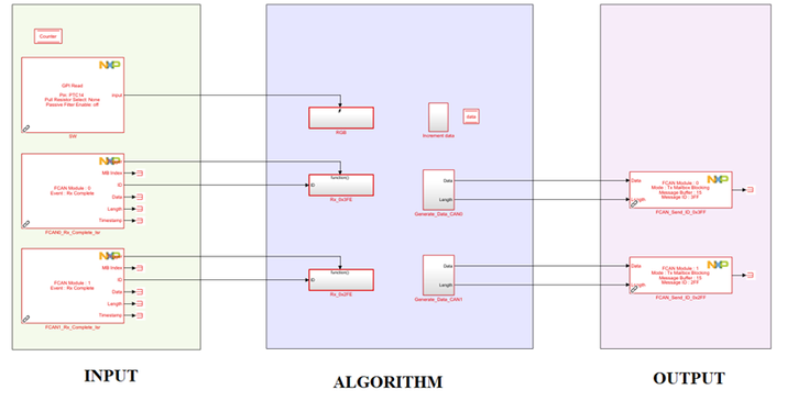
The application is structured in 3 categories as follows:
Input (green area): Hardware-dependent blocks that read/receive values from peripherals
Algorithm (blue area): Hardware-independent blocks that process the values received from Input blocks, runs the algorithm and controls the outputs.
Output (pink area): Hardware-dependent blocks which receive the processed values from the Algorithm blocks.
After all the steps have been followed, the code can be generated, compiled, and deployed on the target.
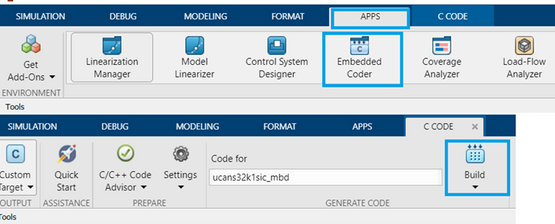
To do so, Go to Simulink -> Apps -> Embedded Coder then click on the Build button.
In the Diagnostic Viewer, the process can be analyzed if there is any error and if the download was successfully completed on the target as in the image below:

Conclusion
In this article we explained how to use the NXP Model-Based Design Toolbox for S32K1xx to handle the UCANS32K1SIC evaluation board. Access to all the board's peripherals was possible in Simulink by using the Model-Based Design Toolbox, an addon which connects the MATLAB and Simulink high level world with the NXP Tools and Hardware.
In this application, we have shown how to control the RGB LED and read the state of the switch; how to display messages on the LCD screen and configure both instances of the CAN communication protocol for sending and receiving messages. We have also added the FreeMASTER communication to monitor or fine-tune the algorithms running on the UCANS32K1SIC board, while the model is available down below.
EdgeLock and NXP are trademarks of NXP B.V. All other product or service names are the property of their respective owners. © 2023 NXP B.V. Arm, Cortex are trademarks and/or registered trademarks of Arm Limited (or its subsidiaries or affiliates) in the US and/or elsewhere. The related technology may be protected by any or all of patents, copyrights, designs and trade secrets. All rights reserved. MATLAB, Simulink, Stateflow and Embedded Coder are registered trademarks and MATLAB Coder, Simulink Coder are trademarks of The MathWorks, Inc. See mathworks.com/trademarks for a list of additional trademarks.