- Forums
- Product Forums
- General Purpose MicrocontrollersGeneral Purpose Microcontrollers
- i.MX Forumsi.MX Forums
- QorIQ Processing PlatformsQorIQ Processing Platforms
- Identification and SecurityIdentification and Security
- Power ManagementPower Management
- Wireless ConnectivityWireless Connectivity
- RFID / NFCRFID / NFC
- Advanced AnalogAdvanced Analog
- MCX Microcontrollers
- S32G
- S32K
- S32V
- MPC5xxx
- Other NXP Products
- S12 / MagniV Microcontrollers
- Powertrain and Electrification Analog Drivers
- Sensors
- Vybrid Processors
- Digital Signal Controllers
- 8-bit Microcontrollers
- ColdFire/68K Microcontrollers and Processors
- PowerQUICC Processors
- OSBDM and TBDML
- S32M
- S32Z/E
-
- Solution Forums
- Software Forums
- MCUXpresso Software and ToolsMCUXpresso Software and Tools
- CodeWarriorCodeWarrior
- MQX Software SolutionsMQX Software Solutions
- Model-Based Design Toolbox (MBDT)Model-Based Design Toolbox (MBDT)
- FreeMASTER
- eIQ Machine Learning Software
- Embedded Software and Tools Clinic
- S32 SDK
- S32 Design Studio
- GUI Guider
- Zephyr Project
- Voice Technology
- Application Software Packs
- Secure Provisioning SDK (SPSDK)
- Processor Expert Software
- Generative AI & LLMs
-
- Topics
- Mobile Robotics - Drones and RoversMobile Robotics - Drones and Rovers
- NXP Training ContentNXP Training Content
- University ProgramsUniversity Programs
- Rapid IoT
- NXP Designs
- SafeAssure-Community
- OSS Security & Maintenance
- Using Our Community
-
- Cloud Lab Forums
-
- Knowledge Bases
- ARM Microcontrollers
- i.MX Processors
- Identification and Security
- Model-Based Design Toolbox (MBDT)
- QorIQ Processing Platforms
- S32 Automotive Processing Platform
- Wireless Connectivity
- CodeWarrior
- MCUXpresso Suite of Software and Tools
- MQX Software Solutions
- RFID / NFC
- Advanced Analog
-
- NXP Tech Blogs
- Home
- :
- Topics
- :
- NXP Designs Knowledge Base
- :
- EMVCo L1 Contactless certification process
EMVCo L1 Contactless certification process
- Subscribe to RSS Feed
- Mark as New
- Mark as Read
- Bookmark
- Subscribe
- Printer Friendly Page
- Report Inappropriate Content
EMVCo L1 Contactless certification process
EMVCo L1 Contactless certification process
This post entry provides a detailed information about the EMVCo L1 certification process for contactless payment devices. The structure is the following:
- EMV Introduction
- Objective
- EMVCo organization
- EMV Technologies
- EMV Contactless specifications
- PCD L1 Type Approval
- EMV Analog L1 PCD Tests
- Environment
- Device Test Environment (DTE)
- Contactless symbol
- Positioning convention
- EMVCo Reference PICC
- Power tests
- Waveform tests
- Reception tests
- Other tests
- EMV Contactless Specs v3.0
- NXP Product portfolio for POS
- Further Information
- Video recorded session
EMV Introduction
Objective
When a company is developing a POS device, there are some challenges to consider for a successful deployment in the market:
- The device needs to have a good performance to provide the client with a good user experience.
- Moreover, the device should be able to operate seamlessly with other devices and cards in the market in a secure and reliable way.
These key characteristics are tackled by the EMV specifications. Summarizing, EMV is a group of specifications for smart payment cards and terminals that were created by EMVCo to guarantee interoperability and acceptance of secure payment transactions. EMV stands for Europay, Mastercard, and Visa, the three companies that originally created the standard. These specifications are now managed by EMVCo, an organization of six members – including Mastercard, UnionPay, Visa, AmEx, Discover, and JCB.
EMVCo organization
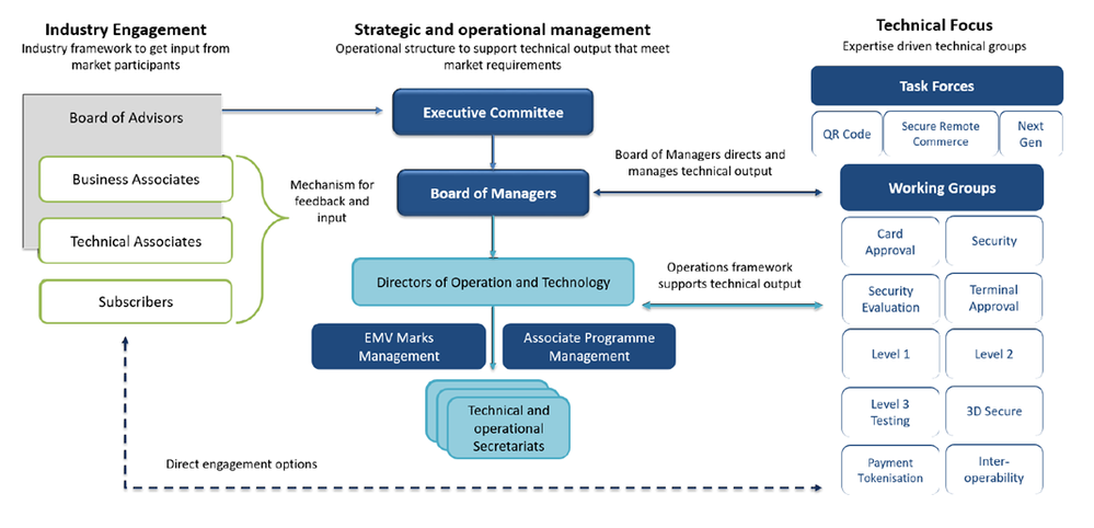
We can see in the figure below the structure of the organization. EMVCo is managed by the Board of Managers that consists of two representatives of every member of the organization. On top of the Board of Managers, the Executive Committee provides guidance on the group’s long-term strategy.
From a more technical point-of-view, it is organized in several Working Groups, each of them dedicated to specific topics. EMVCo also has the Associates Program, so key industry stakeholders can provide input and feedback to the Board of Managers, Executive Committee, and Working Groups.
EMV Technologies
EMV specifications encompass a wide range of technologies, including:
- Contact chip technology, where smartcards and readers provide with cryptographical security advantages in comparison with the traditional magnetic stripe.
- EMV specifications also regulate contactless payment devices based on NFC technology.
- Mobile Transactions where the mobile phone would play the role of a contactless device.
- The QR code technology, where the transaction can be made using a QR reader.
- Payment tokenization, that enables to perform transactions without compromising sensible card information.
- And other technologies like Secure Remote Commerce, 2nd Gen or 3-D Secure.
EMV Contactless specifications
EMV Contactless specifications is now on version 2.6 but planning to move to version 3.0 by the end of the year.
The EMV Contactless specifications are structured in three books and the Contactless Interface Specifications that substitutes the Book D from previous versions of the specs.
- The Book A describes the overall architecture of the system, and the instructions involved in the communication between the entry point and the kernel.
- The Book B addresses the specifications regarding the Entry Point, which is the piece of sw in charge of the transaction pre-processing, or protocol activation among other tasks.
- Book C consists of 6 different levels for each of the kernels that are defined in the specifications.
- The EMV Contactless Interface Specifications describe the minimum set of functionalities that are required for the correct operation between the PICCs and the PCD.
In addition we will mention other relevant documents like:
- The PCD Test Bench and Test Case Requirements, that describes the test cases that are carried out by the testing laboratory in order to evaluate the devices. Note that there are 2 different documents, one for the Analog L1 tests and another one for the Digital tests.
- Another document describes the Device Test Environment, which is the software needed to control the device during the testing phase
- Another document describes the requirements regarding the Contactless symbol that should appear in all EMVCo Contactless POS in the market.
PCD L1 Type Approval
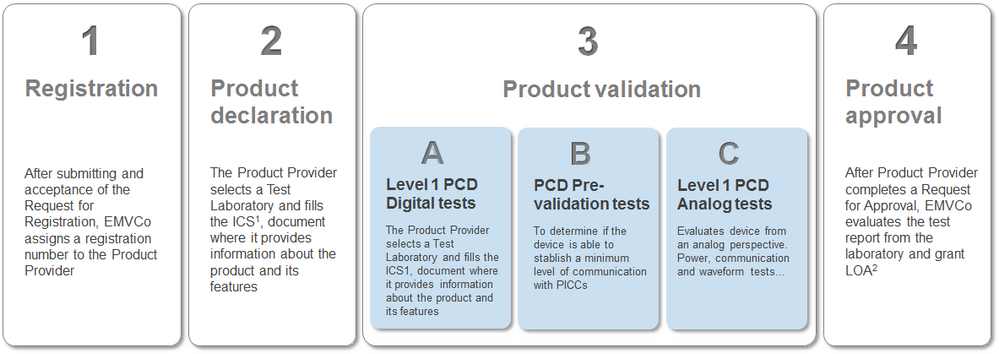
The following diagram summarizes the process for the PCD L1 Type Approval:
In the first step the Product Provider shall submit a Request for Registration form to EMVCo. Once EMVCo reviews and accepts the form, the product provider will receive a contract that has to be signed. Upon reception of this contract, EMVCo will assign a product provider registration number.
In the second step the Product Provider will choose a Test Laboratory and complete a document called Implementation Conformance Statement in which it provides detailed information about the device and its features.
The third step is the Product Validation phase. In this phase the laboratory performs the product testing, where the device goes through a set of tests to evaluate the digital and analog performance.
In a final phase and considering the test reports from the Laboratory, the Product Provider might decide to send the product to EMVCo for approval. In that case, EMVCo would analyze the tests reports and grant with a Letter of Approval in case the reports demonstrate sufficient product conformance.
In our case we are going to focus on the Analog L1 PCD tests.
EMV Analog L1 PCD Tests
Environment
Before going directly to the actual set of tests, it worth it to explain some components about the testing environment to better understand the testing procedure. We have the following elements:
- Device Test Environment
- Contactless symbol
- Positioning conventions
- EMVCo Reference PICC
Device Test Environment (DTE)
The Device Test Environment is a software application that is used to control the device under evaluation during the whole testing process. This application has to be developed by the product provider and shall be implemented in compliance with a set of requirements defined in the specifications. The software is submitted to the test laboratory along with the samples of the device under certification. The DTE shall implement different applications or modes of operation that would be used depending on the testing scenario. These application are:
- PCD Controls: It allows the test operator to execute single basic commands from the ISO14443 standard (Carrier ON/OFF, WUPA, WUPB,..)
- Pre-validation application: This application is used to test the communication of the device with a set of actual EMV compliant cards.
- Loopback application: It is used to test the device for the majority of the Analog and Digital L1 PCD Tests. In this case the reader is communicating with a Card simulator connected to a reference antenna.
- Transaction send application: This application can be used by the laboratory to evaluate the compliancy of the device with the waveform requirements defined for the Analog L1 PCD Tests. The main characteristic of this mode of operation is that the device sends a sequence of commands without waiting the responses from the PICC.
Contactless symbol
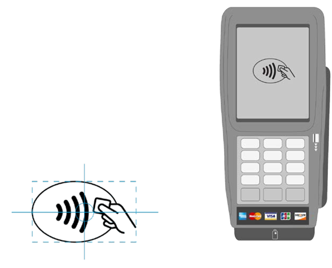
The contactless symbol is the logo that you can see in the lower image. It helps the user identify the area in the Point Of Sale where he has to tap the card in order to trigger the transaction. This symbol has to be visible in the device surface or screen before and during the transaction. The Contactless symbol is extremely important for the testing procedure as it marks the reference point for all the positions that the device should be tested.
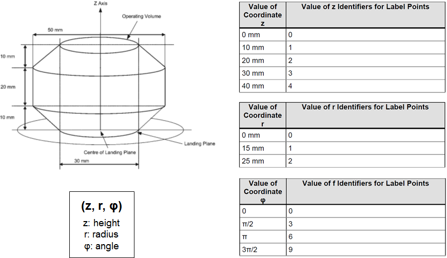
Using this reference point EMVCo defines an operating volume.
Positioning convention
All test position are included in this operating volume. Depending on the test case, it will be run in one or more positions. Every position is expressed with a set of 3 coordinates or parameters, representing the height, the radius, and the angle respectively.
In the figure above you can see the operating volume along with the different values that each parameter can have.
EMVCo Reference PICC
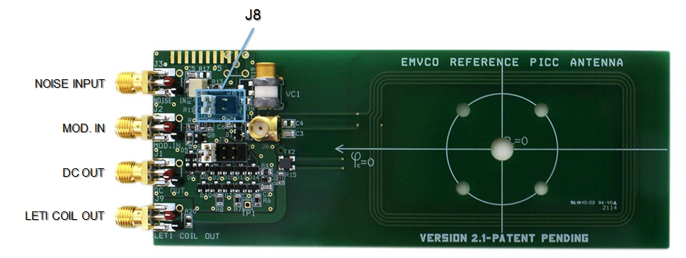
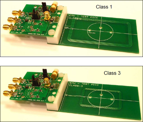
The EMVCo Reference PICC is the reference antenna used to communicate with the PCD under test. It has 4 ports and 2 jumpers that are used to configure the PICC for different purposes. For example, jumper 8 is used to select between linear and non-linear load depending on the type of tests that are performed.
In the same line, the MOD IN port where a Signal Generator will inject a certain modulation to emulate a PICC response. The DC OUT port is used to measure the voltage level in the power tests and the LETI COIL OUT is used to measure the waveform tests among others. In the figure below you can also see the reference point of the antenna where the two white lines crossed:
Power tests
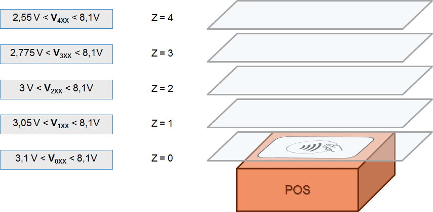
The power tests are evaluated in all positions with the purpose of guaranteeing that the device is emitting enough field in all the positions. Depending on the height the limiting values will differ. In the figure below you can see the different planes with the respective limiting values.
The critical positions for the power tests are usually the outer positions for plane z=4 and z=3 where the voltage measured may not be strong enough to pass the tests.
On top of that and depending on the transmission configuration used, it can also happen that the voltage measured at positions (1, 0, 0) and (0, 0, 0) can exceed the maximum level.
Waveform tests
The purpose of the waveform tests is to evaluate the wave shape of the modulation used in the commands from the PCD. That way, if the wave shape fits with the requirements an EMVCo compliant PICC would not have any problem understanding the commands sent by the PCD.
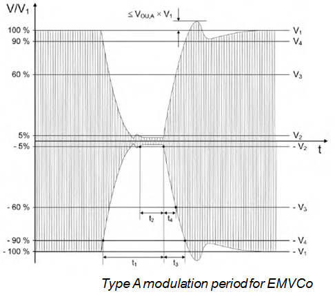
The waveform evaluation for Type A modulation include the following test cases:
- t1 (TB121)
- Monotonic Decrease (TB122)
- Ringing (TB123)
- t2 (TB124)
- t3 and t4 (TB125)
- Monotonic Increase (TB126)
- Overshoot (TB127)
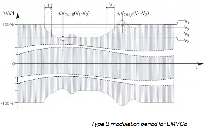
In the same way, the Type B test cases are the following:
- Modulation Index (TB121)#
- Fall time (TB122)
- Rise time (TB123)
- Monotonic Increase (TB124)
- Monotonic Decrease (TB125)
- Overshoots (TB126)
- Undershoots (TB127)
Reception tests
The objective of the communication or responsiveness tests is to guarantee that the PCD is able to properly finish a transaction when the response of the PICC is in the limits of the specifications in terms of amplitude and polarity.
That way we find 4 different tests:
- Minimum load modulation, positive polarity (Tx131)
- Maximum load modulation, positive polarity (Tx133)
- Minimum load modulation, negative polarity (Tx135)
- Maximum load modulation, negative polarity (Tx137)
In the two figures below we can easily check the difference in the load modulation level between the oscilloscope capture for the Tx131 and the Tx133.
Other tests
Besides the power, waveform and communication tests there are other tests included in the EMVCo Analog L1 Test cases. Here is the list of these other tests:
- Carrier frequency (TAB112)
- Field resetting (TAB113)
- Power off (TAB114)
- Polling sequence (TAB115)
- FDTA PICC (TA139)
- BitRate (TA141 & TB141)
- BitCodingPCD (TA142 & TB142)
- BitCodingPICC (TA143 & TB146)
- BitBoundaries (TB147)
- TFSOFF (TB145 & TB148)
EMV Contactless Specs v3.0
The most important change is that the tests will no longer be carried out with one specific EMVCo reference PICC but with three. The first two are Class 1 antennas tuned to 16.1MHz and 13.56MHz, and the third reference PICC is a Class 3 antenna tuned to 13.56MHz.
This is important since the device will need to pass the test for 3 different antennas, making the testing process between 2 and 3 times slower and the tuning of the device more difficult than for the 2.6 version of the specs.
Other changes are a second different load for the linear load tests and the modifications of some waveform tests limits.
NXP Product portfolio for POS
The product portfolio that NXP offers for contactless POS device includes three main chips:
- CLRC663 plus: EMVCo 2.6 ready chip compliant both for analog and digital L1 requirements. The CLRC663 plus is able to work with a transmitter current of 350 mA and a limiting value of 500 mA. This feature allows us to increase the field strength radiated and overcome power issues because of the design of the POS or the antenna.
- PN5180: The PN5180 chip is also an EMVCo compliant frontend, that supports highly innovative and unique features like the Dynamic Power Control that optimizes the RF performance even under detuned antenna conditions. Other features are the Adaptative Waveform Control or the Adaptative Receiver Control to automatically adjust the transmitter modulation or the receiver parameters. These and many other features turn the PN5180 into the best NFC frontend in the market.
- PN7462: It supports contact and contactless interface in the same chip. It is an NFC controller, so includes an MCU with a configurable host interface. For the contactless interface, it implements similar functionalities as the PN5180, like the Dynamic Power Control, the Adaptative Receiver Control, and the Adaptative Waveform Control.
Further Information
You can find more information about NFC in:
- Our NFC everywhere portal: https://www.nxp.com/nfc
- You can ask your question in our technical community: https://community.nxp.com/community/identification-security/nfc
- You can look for design partners: https://nxp.surl.ms/NFC_AEC
- And you can check our recorded training: http://www.nxp.com/support/online-academy/nfc-webinars:NFC-WEBINARS
