- Forums
- Product Forums
- General Purpose MicrocontrollersGeneral Purpose Microcontrollers
- i.MX Forumsi.MX Forums
- QorIQ Processing PlatformsQorIQ Processing Platforms
- Identification and SecurityIdentification and Security
- Power ManagementPower Management
- Wireless ConnectivityWireless Connectivity
- RFID / NFCRFID / NFC
- MCX Microcontrollers
- S32G
- S32K
- S32V
- MPC5xxx
- Other NXP Products
- S12 / MagniV Microcontrollers
- Powertrain and Electrification Analog Drivers
- Sensors
- Vybrid Processors
- Digital Signal Controllers
- 8-bit Microcontrollers
- ColdFire/68K Microcontrollers and Processors
- PowerQUICC Processors
- OSBDM and TBDML
- S32M
-
- Solution Forums
- Software Forums
- MCUXpresso Software and ToolsMCUXpresso Software and Tools
- CodeWarriorCodeWarrior
- MQX Software SolutionsMQX Software Solutions
- Model-Based Design Toolbox (MBDT)Model-Based Design Toolbox (MBDT)
- FreeMASTER
- eIQ Machine Learning Software
- Embedded Software and Tools Clinic
- S32 SDK
- S32 Design Studio
- GUI Guider
- Zephyr Project
- Voice Technology
- Application Software Packs
- Secure Provisioning SDK (SPSDK)
- Processor Expert Software
-
- Topics
- Mobile Robotics - Drones and RoversMobile Robotics - Drones and Rovers
- NXP Training ContentNXP Training Content
- University ProgramsUniversity Programs
- Rapid IoT
- NXP Designs
- SafeAssure-Community
- OSS Security & Maintenance
- Using Our Community
-
- Cloud Lab Forums
-
- Knowledge Bases
- ARM Microcontrollers
- i.MX Processors
- Identification and Security
- Model-Based Design Toolbox (MBDT)
- QorIQ Processing Platforms
- S32 Automotive Processing Platform
- Wireless Connectivity
- CodeWarrior
- MCUXpresso Suite of Software and Tools
- MQX Software Solutions
-
- Home
- :
- RFID / NFC
- :
- NFC
- :
- Re: nhs3152 adc problem
nhs3152 adc problem
nhs3152 adc problem
dear sir
i encounter a question about test the battery voltage with the ADC function .
2 my source about test the vcc voltage code is below
static uint16_t Get_current_adc(void)
{
//int adc_max=0xfff;
int adcInput=0;
int total_adc=0;
//! [adcdac_nss_example_3]
Chip_IOCON_SetPinConfig(NSS_IOCON, IOCON_ANA0_4, IOCON_FUNC_1);
Chip_ADCDAC_Init(NSS_ADCDAC0);
Chip_ADCDAC_SetMuxADC(NSS_ADCDAC0, ADCDAC_IO_ANA0_4);
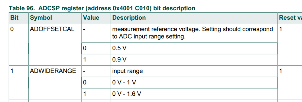
Chip_ADCDAC_SetInputRangeADC(NSS_ADCDAC0, ADCDAC_INPUTRANGE_WIDE);
Chip_ADCDAC_SetModeADC(NSS_ADCDAC0, ADCDAC_CONTINUOUS);
Chip_ADCDAC_StartADC(NSS_ADCDAC0);
int max,min;
total_adc=max=min=0;
for(int i=0;i<10;i++)
{
adcInput = Chip_ADCDAC_GetValueADC(NSS_ADCDAC0);
total_adc+=adcInput;
if(max<adcInput)
max=adcInput;
else if(min>adcInput)
min=adcInput;
}
Chip_ADCDAC_StopADC(NSS_ADCDAC0);
total_adc=total_adc-max-min;
//get the average value
total_adc=total_adc/8;
//get the caculate from https://community.nxp.com/message/1119718#comment-1120963
//output in mV = ((native value - native offset) * internal operating voltage / steps per uV) + offset
//native offset=2048,internal voltage = 1.2V,gain (steps per uV) = 2730,offset = 0.9V
adcInput=(total_adc-2048)*1200/2730+900;// get the test point voltage ,unit is mv
//convert the test point voltage to VCC voltage
adcInput=adcInput*5/2;
return (uint16_t)adcInput;
/* Further handling of the threshold breach. */
}
my question is :
- how can i get these value ?i get from this value in another question ,but i do not no why ?i can not find it in spec ...native offset=2048,internal voltage = 1.2V,gain (steps per uV) = 2730,offset = 0.9V
- my ADC value adcInput change rapidly,it is not a stable value ,
for example ,i get the voltage VCC by multimeter is 3.0V
but ,i tried 10 times test the value ,and get the adcInput = Chip_ADCDAC_GetValueADC(NSS_ADCDAC0);read from the register is below .
| Header 1 | Header 1 | Header 2 | Header 3 | Header 4 | Header 5 | Header 6 | Header 7 | Header 8 | Header 9 |
|---|---|---|---|---|---|---|---|---|---|
| adcInput(mv) | 2695 | 2677 | 2573 | 2596 | 2578 | 2676 | 2597 | 2670 | 2630 |
| VCC(mv) | 2960 | 2941 | 2826 | 2852 | 2832 | 2940 | 2853 | 2933 | 2889 |
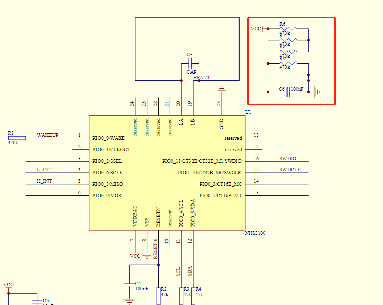
can you give me some advise ?is there anything wrong with my schematic ?
is there anything wrong with my design formula ?
Hi,
It's a bit confusing to use a NHS3100 symbol in your schematics. - a good thing the digital pins are identical to the NHS3152 :-)
When the debug connector is still attached, a lot of noise is injected. Is it possible you measured those numbers within a debug session? If so, can you repeat your measurements without a debug session and without the LPC-Link2 debugger board connected to the NHS3152 IC?
Your fitting parameters used in the formula adcInput=(total_adc-2048)*1200/2730+900 do not ring a bell for me. Can you try to recall how/when/where you received those?
After the weekend, I will try and see if I can find other fitting parameters - we surely must have done this before, I need to check if I can find a trace of that somewhere...
Kind regards,
Dries.
dear dries
thank you for your reply .
i am sorry that i make a mistake in the schematic ,i use 3152 not 3100 in my test .
- the data ADC value that i test is not in debug mode without LPC-LIN2,i use CR2032 instead .
- is there anything wrong in my bleeder circuit ?
the formula adcInput=(total_adc-2048)*1200/2730+900
i get the formula from https://community.nxp.com/message/1119718#comment-1120963 this document that you replied before
- can you give me some advise on test ADC value or any demo design ?
yours
xuejiao
Hi,
The formula given was derived from an early sample, and does not accurately reflect the state of the released ICs.
This formula provides a better conversion for production ICs:
adc_input_voltage = (native_value * 1.2V) / 2825 + 0.09V
(Of course, for your schematics, you need to retain your multiplier 2.5 as well).
Regarding reference design: we have a therapy adherence board available in our sample store, which uses resistive measurements (a.o. using the ADC) to keep track of pill intakes. The full schematics and layout is available in our SDK under <SDK>/docs/NHS3152 Therapy Adherence.zip
More information here: https://www.nxp.com/pages/:NHS3152THADADK
Kind regards,
Dries.
dear sir
i am sorry to trouble you again !
first :
i still confused about the formula you offered before ,how do you get the formula ?
adc_input_voltage = (native_value * 1.2V) / 2825 + 0.09V
how to use reference voltage / ADC resolution 12 bit and input range get the formula ?
second :
i have another question about ADC like before ,my schematic is still the picture like before ,i get the ADC raw value from the register now ,and calculate the value average about 10 times .but there is still about 15 --20 raw data fluctuation . i have no idea how to deal with the fluctuation ,can you give me some advise ?
Hi,
1
The ADC is not linear at the extremities, causing a slightly steeper slope of the conversion from raw to voltage. The formula takes this into account.
2
A 20 raw data fluctuation corresponds to ~8.5 mV, which is not that much. There is noise on the voltage input, and the IC being active also causes small fluctuations. You can use a scope to measure more precisely the voltage, as a multimeter is only showing averages. Perhaps best is to configure the scope in AC-coupled input mode to measure the ripple on the battery directly. You can also bring out a signal to synchronize the scope measurements with the ADC conversions.
Best,
Dries.

