
- Forums
- Product Forums
- General Purpose MicrocontrollersGeneral Purpose Microcontrollers
- i.MX Forumsi.MX Forums
- QorIQ Processing PlatformsQorIQ Processing Platforms
- Identification and SecurityIdentification and Security
- Power ManagementPower Management
- Wireless ConnectivityWireless Connectivity
- RFID / NFCRFID / NFC
- Advanced AnalogAdvanced Analog
- Neural Processing UnitsNeural Processing Units
- MCX Microcontrollers
- S32G
- S32K
- S32V
- MPC5xxx
- Other NXP Products
- S12 / MagniV Microcontrollers
- Powertrain and Electrification Analog Drivers
- Sensors
- Vybrid Processors
- Digital Signal Controllers
- 8-bit Microcontrollers
- ColdFire/68K Microcontrollers and Processors
- PowerQUICC Processors
- OSBDM and TBDML
- S32M
- S32Z/E
-
- Solution Forums
- Software Forums
- MCUXpresso Software and ToolsMCUXpresso Software and Tools
- CodeWarriorCodeWarrior
- MQX Software SolutionsMQX Software Solutions
- Model-Based Design Toolbox (MBDT)Model-Based Design Toolbox (MBDT)
- FreeMASTER
- eIQ Machine Learning Software
- Embedded Software and Tools Clinic
- S32 SDK
- S32 Design Studio
- GUI Guider
- Zephyr Project
- Voice Technology
- Application Software Packs
- Secure Provisioning SDK (SPSDK)
- Processor Expert Software
- Generative AI & LLMs
-
- Topics
- Mobile Robotics - Drones and RoversMobile Robotics - Drones and Rovers
- NXP Training ContentNXP Training Content
- University ProgramsUniversity Programs
- Rapid IoT
- NXP Designs
- SafeAssure-Community
- OSS Security & Maintenance
- Using Our Community
-
- Cloud Lab Forums
-
- Knowledge Bases
- ARM Microcontrollers
- i.MX Processors
- Identification and Security
- Model-Based Design Toolbox (MBDT)
- QorIQ Processing Platforms
- S32 Automotive Processing Platform
- Wireless Connectivity
- CodeWarrior
- MCUXpresso Suite of Software and Tools
- MQX Software Solutions
- RFID / NFC
- Advanced Analog
- Neural Processing Units
-
- NXP Tech Blogs
- Home
- :
- RFID / NFC
- :
- NFC
- :
- Re: How to Set and Reset I2C_LOCKED bit in NS_REG register inside Session Register, from I2C interface
How to Set and Reset I2C_LOCKED bit in NS_REG register inside Session Register, from I2C interface
- RSS フィードを購読する
- トピックを新着としてマーク
- トピックを既読としてマーク
- このトピックを現在のユーザーにフロートします
- ブックマーク
- 購読
- ミュート
- 印刷用ページ

- 新着としてマーク
- ブックマーク
- 購読
- ミュート
- RSS フィードを購読する
- ハイライト
- 印刷
- 不適切なコンテンツを報告
Hi Sir / Madam,
I encounter communication problem when NXP NTAG 1K communicate with peer NFC device.
My problem is I am not able to Set or Reset I2C_LOCKED bit in NS_REG register inside Session Register. From datasheet (NT3H1101/NT3H1201.pdf, page 27/65, Table 14), this bit can be Read and Write by I2C interface.
During peer NFC device(RF interface) has read the mirror SRAM in NXP NTAG 1K, NS_REG = 0xA9 or 0x29, NC_REG=0x7E. For NS_REG = 0xA9, it means NDEF_DATA_READ = 1b, RF_LOCKED = 1b, SRAM_RF_READY=1b and RF_FIELD_PRESENT=1b. I can understand SRAM_RF_READY=1b because RF interface is read from Mirror SRAM, Not Mapped SRAM. But, may I know why Memory is still lock to RF, as shown in RF_LOCKED = 1b ? Doesn't it will change to RF_LOCKED = 0b and I2C_LOCKED = 1b ? Because RF interface has read the last page of Mirror SRAM Block, as this is correctly shown in NDEF_DATA_READ = 1b.
Is the above phenomena also caused by RF interface reading from Mirror SRAM, NOT Mapped SRAM ? Then, may I know after RF interface has read the Mirrored SRAM, how I2C interface able to write data again ?
As an attempt to solve above problem, I have try to manually write 1b to I2C_LOCKED. But I am not able to write on this bit although datasheet mention that this bit is R&W from I2 interface.
During this experiment and observation, RF field is stable and constantly provided. In addition, Pass through and its direction is maintained as shown in NC_REG=0x7E reading. Also, RF is successfully reading on the correctly configure SRAM MIRROR BLOCK address.
Please advice soon.
Thank you very much for your help and advice.
Cheers,
KF Choong
Skype: ohchat12
解決済! 解決策の投稿を見る。

 Jorge_Gonzalez
- 新着としてマーク
- ブックマーク
- 購読
- ミュート
- RSS フィードを購読する
- ハイライト
- 印刷
- 不適切なコンテンツを報告
Hello KF Choong,
I am sorry for the delay to revise your question.
Pay attention that SRAM Memory Mirror mode cannot be combined with Pass-through mode (either one enabled, not both).
While RF_LOCKED = 1, from the I2C interface you can only read registers, but not write.
If Pass-through is enabled as in your case, with SRAM_RF_READY = 1 and PTHRU_DIR = 0 (direction from I2C to RF) , the RF_LOCKED and SRAM_RF_READY bits will be reset to 0b when the terminator block/page of the SRAM is read from the RF side.
Maybe the attached presentation about Pass-through mode can bring some clarity.
Best Regards!
Jorge Gonzalez
Jorge_Gonzalez
- 新着としてマーク
- ブックマーク
- 購読
- ミュート
- RSS フィードを購読する
- ハイライト
- 印刷
- 不適切なコンテンツを報告
Hello KF Choong,
I am sorry for the delay to revise your question.
Pay attention that SRAM Memory Mirror mode cannot be combined with Pass-through mode (either one enabled, not both).
While RF_LOCKED = 1, from the I2C interface you can only read registers, but not write.
If Pass-through is enabled as in your case, with SRAM_RF_READY = 1 and PTHRU_DIR = 0 (direction from I2C to RF) , the RF_LOCKED and SRAM_RF_READY bits will be reset to 0b when the terminator block/page of the SRAM is read from the RF side.
Maybe the attached presentation about Pass-through mode can bring some clarity.
Best Regards!
Jorge Gonzalez
- 新着としてマーク
- ブックマーク
- 購読
- ミュート
- RSS フィードを購読する
- ハイライト
- 印刷
- 不適切なコンテンツを報告
Hi Jorge,
May I know where can I download the firmware code for NTAG I2C ?
I have search NXP portal and cannot find it.
I am looking for the code for BOOL NTAG_WaitForEvent(NTAG_HANDLE_T ntag, NTAG_EVENT_T event, uint32_t timeout_ms). And all its related functions, which is in embedded in NXP MCU. For example:
HAL_ISR_SleepWithTimeout(ntag->isr, timeout_ms);,..., HAL_ISR_RegisterCallback(ntag->isr, ISR_LEVEL_HI, NULL, NULL);. These are the command for NXP MCU.
Please help.
Thank you.
Cheers,
KF
Jorge_Gonzalez
- 新着としてマーク
- ブックマーク
- 購読
- ミュート
- RSS フィードを購読する
- ハイライト
- 印刷
- 不適切なコンテンツを報告
Hi KF Choong,
You can download the firmware from NTAG I2C (NT3H1101_NT3H1201) product page, under "Software and tools" tab:
Regards!
Jorge Gonzalez
- 新着としてマーク
- ブックマーク
- 購読
- ミュート
- RSS フィードを購読する
- ハイライト
- 印刷
- 不適切なコンテンツを報告
Hi Jorge,
Once again, many thanks for all your helps and replies.
I think my project is almost done although some minor issues are pending.
I really appreciate your help and you have been a great NFC consultant.
Thank you very much.
Cheers,
KFChoong
- 新着としてマーク
- ブックマーク
- 購読
- ミュート
- RSS フィードを購読する
- ハイライト
- 印刷
- 不適切なコンテンツを報告
Hi Jorge,
For configuration FD_On=11b and FD_OFF=11b, using mirror SRAM, I configure for RF interface write initially. Then, RF interface ( Peer NFC) starting to write to mirror SRAM (User memory) of NTAG. When RF interface finished writing, the FD Pin does not toggle. In additional, there is also no change in Memory lock bit and SRAM ready bit. May I know how can I get any kind of notice, especially on FD Pin, when RF have finished writing ? I need this notice to create an interrupt for the microcontroller attached to NTAG.
Please write soon.
Thank you very much.
Cheers,
KF Choong
- 新着としてマーク
- ブックマーク
- 購読
- ミュート
- RSS フィードを購読する
- ハイライト
- 印刷
- 不適切なコンテンツを報告
Hi Jorge,
Happy New Year 2017 and may you and your family have a great year ahead !
And, I have forgotten, Merry Christmas too :smileyhappy:
Cheers,
KeanFatt
- 新着としてマーク
- ブックマーク
- 購読
- ミュート
- RSS フィードを購読する
- ハイライト
- 印刷
- 不適切なコンテンツを報告
HI Jorge,
I encounter some problem during RF read and write. May I have your opinion on the following questions :
(1) Every time I do RF write or read I need to do initialisation cycle as shown in figure 5 - RF communication principle of NTAG I2C.
If I am not doing this, I will not be able to write correctly or after written, the I2C SRAM Ready bit is not toggle.
(2) Every time after read session register, I have to do twice initialisation in order for the subsequent read and write works correctly.
I do twice initialisation is because the first REQA command which ST95 send to NTAG will fail, timeout. Then the second REQA will PASS. May I know why ?
(3) I have encounter Pass through has been OFF even though RF Field is constantly ON. And, there is no code to switch Pass through.
(4) When there is a field ON initialisation after read session register, the communication of ST95 and NTAG will behave : success, timeout, timeout, success, timeout, success, timeout,......,
In view of the above code, I have try to dig into some article of REQA, but still unable to get any clue. May I ask what is inside of NTAG hardware architecture ? any buffer ? How the REQA actually works inside NTAG ? Anyway I can tap the internal activities of NTAG chip ?
Also, may I ask what is the purpose or use of WDT_MS register, WDT_LS register and I2C_CLOCK_STR register. The explanation is less detail for these features. Will WDT_MS register, WDT_LS register and I2C_CLOCK_STR register shut down the NTAG chip automatically, which cause it need to re-initialisation again ?
Please help me on the above issues. your help is very much appreciated.
Thank you very much.
Cheers,
KF
- 新着としてマーク
- ブックマーク
- 購読
- ミュート
- RSS フィードを購読する
- ハイライト
- 印刷
- 不適切なコンテンツを報告
Hi Jorge,
Many thanks for your prompt action.
Thank you very much.
Cheers,
KF Choong
- 新着としてマーク
- ブックマーク
- 購読
- ミュート
- RSS フィードを購読する
- ハイライト
- 印刷
- 不適切なコンテンツを報告
Hi Jorge,
I have plan to do an Interrupt approach.
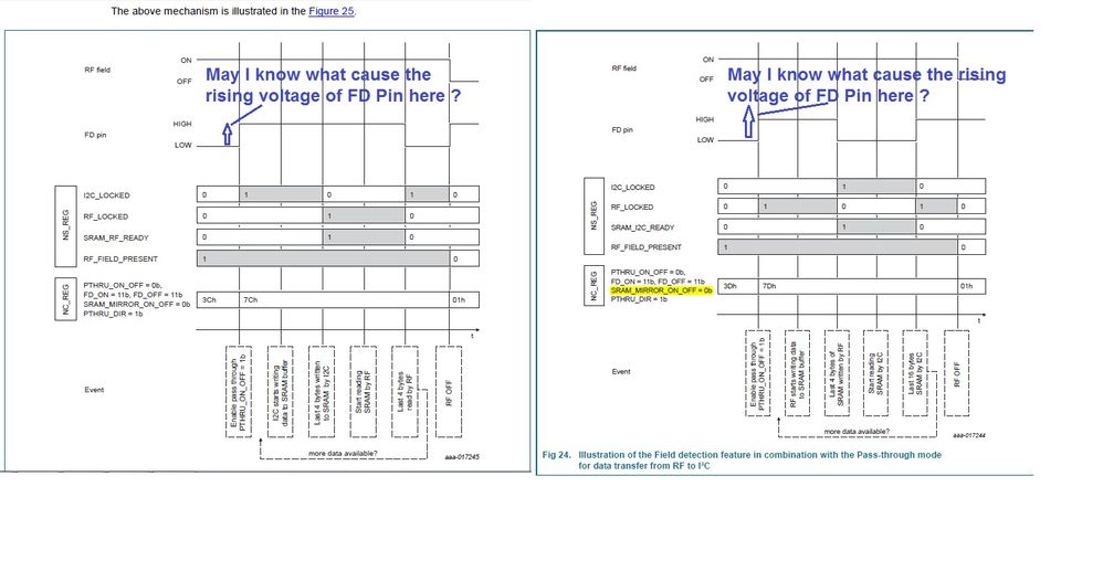
When reviewing the diagram on Datasheet, I have some doubts as attached on the JPEG file, on the FD Pin behaviour when configure to FD_ON = 11b and FD_OFF = 11b.
Would you please help me out on this ?
Thank you very much.
Cheers,
KF Choong
Jorge_Gonzalez
- 新着としてマーク
- ブックマーク
- 購読
- ミュート
- RSS フィードを購読する
- ハイライト
- 印刷
- 不適切なコンテンツを報告
Hi KF Choong,
In your pictures you can see the events in the dotted line boxes below. In both cases the FD pin rises when enabling the Pass-through mode while FD_OFF = 11b and FD_ON = 11b. In fact that rising edge should be ignored by the MCU. It just means that the pin is going to OFF mode and preparing to signal the next upcoming event with a falling edge.
Regards!
Jorge Gonzalez
- 新着としてマーク
- ブックマーク
- 購読
- ミュート
- RSS フィードを購読する
- ハイライト
- 印刷
- 不適切なコンテンツを報告
Hi Jorge,
Thank you for your reply.
I just realise that this pin is a pull down pin and I will ignore this signal.
Thank you.
Cheers,
KF Choong
- 新着としてマーク
- ブックマーク
- 購読
- ミュート
- RSS フィードを購読する
- ハイライト
- 印刷
- 不適切なコンテンツを報告
Hi Jorge,
I am sorry for the late reply, wa assign to another urgent project.
Many thanks for your answer. I will explore again on some features offer by Pass Through Mode.
For your information, I am able to configure for Pass through mode and at the same time, having the choices for Mirror and Mapped SRAM on RF interface.
Well thanks a lot. :smileyhappy:
Cheers,
KF Choong
