- Forums
- Product Forums
- General Purpose MicrocontrollersGeneral Purpose Microcontrollers
- i.MX Forumsi.MX Forums
- QorIQ Processing PlatformsQorIQ Processing Platforms
- Identification and SecurityIdentification and Security
- Power ManagementPower Management
- Wireless ConnectivityWireless Connectivity
- RFID / NFCRFID / NFC
- MCX Microcontrollers
- S32G
- S32K
- S32V
- MPC5xxx
- Other NXP Products
- S12 / MagniV Microcontrollers
- Powertrain and Electrification Analog Drivers
- Sensors
- Vybrid Processors
- Digital Signal Controllers
- 8-bit Microcontrollers
- ColdFire/68K Microcontrollers and Processors
- PowerQUICC Processors
- OSBDM and TBDML
- S32M
-
- Solution Forums
- Software Forums
- MCUXpresso Software and ToolsMCUXpresso Software and Tools
- CodeWarriorCodeWarrior
- MQX Software SolutionsMQX Software Solutions
- Model-Based Design Toolbox (MBDT)Model-Based Design Toolbox (MBDT)
- FreeMASTER
- eIQ Machine Learning Software
- Embedded Software and Tools Clinic
- S32 SDK
- S32 Design Studio
- GUI Guider
- Zephyr Project
- Voice Technology
- Application Software Packs
- Secure Provisioning SDK (SPSDK)
- Processor Expert Software
-
- Topics
- Mobile Robotics - Drones and RoversMobile Robotics - Drones and Rovers
- NXP Training ContentNXP Training Content
- University ProgramsUniversity Programs
- Rapid IoT
- NXP Designs
- SafeAssure-Community
- OSS Security & Maintenance
- Using Our Community
-
- Cloud Lab Forums
-
- Knowledge Bases
- ARM Microcontrollers
- i.MX Processors
- Identification and Security
- Model-Based Design Toolbox (MBDT)
- QorIQ Processing Platforms
- S32 Automotive Processing Platform
- Wireless Connectivity
- CodeWarrior
- MCUXpresso Suite of Software and Tools
- MQX Software Solutions
- RFID / NFC
-
- Home
- :
- モデルベース・デザイン・ツールボックス(MBDT)
- :
- モデルベース・デザイン・ツールボックス(MBDT)
- :
- Re: MotorGD pre-drive config problems
MotorGD pre-drive config problems
- RSS フィードを購読する
- トピックを新着としてマーク
- トピックを既読としてマーク
- このトピックを現在のユーザーにフロートします
- ブックマーク
- 購読
- ミュート
- 印刷用ページ
- 新着としてマーク
- ブックマーク
- 購読
- ミュート
- RSS フィードを購読する
- ハイライト
- 印刷
- 不適切なコンテンツを報告
@adriantudor Hello
I have set the config as your advice,
but the GD3000 also did not work.
I found that the J1-1(GD_EN) was always zero.
Could you test my simulink(test1) and check if the same problems appear?
And I added the GD_EN to the stateflow,but the deadtime was still 15us.
Could you help me check the model(test 2) and find the reason ?
best regards
hao
解決済! 解決策の投稿を見る。
- 新着としてマーク
- ブックマーク
- 購読
- ミュート
- RSS フィードを購読する
- ハイライト
- 印刷
- 不適切なコンテンツを報告
@haoxue1027 Hi Hao,
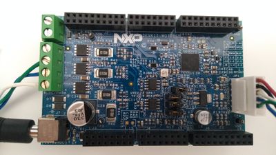
Please see my jumpers setup and if you want to try it (this one it's working with default pins and SPI0). I want to mention that this setup it's working for me but you have to remove 2 resistors from DEVKIT-MOTORGD : R70 and R73. The reason to remove those two resistors is that the output impedance of the level shifter it affect the signal if at the output is connected a pullup or pulldown resistor lower than 50kohm.
Your PWM output it's normal.
Best regards,
Adrian
- 新着としてマーク
- ブックマーク
- 購読
- ミュート
- RSS フィードを購読する
- ハイライト
- 印刷
- 不適切なコンテンツを報告
Hi @haoxue1027 ,
Unfortunately, I don't have Rev. E at this moment, but, I will try to help you.
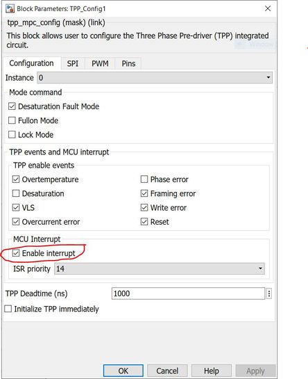
First thing if you don't use the TPP interrupt, please disable it (uncheck the red box).
Then check jumpers: J28, J22, J31 must be set according to your setup (1-2 for 3.3V or 2-3 for 5V),
J29 - off, J23 - off. And be sure that you power the DEVKIT_MOTORGD using J7 connector placed on MOTORGD.
Please let me know if that helps.
Best regards,
Adrian
- 新着としてマーク
- ブックマーク
- 購読
- ミュート
- RSS フィードを購読する
- ハイライト
- 印刷
- 不適切なコンテンツを報告
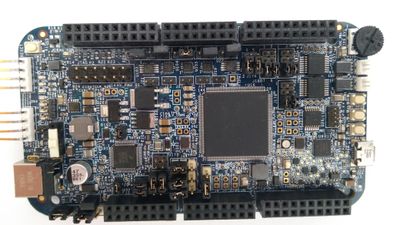
NXP Ultra-Reliable MCUs Development Platforms are a small, cost-effective evaluation, and development system for quick application, prototyping, and demonstration using Ultra-Reliable Automotive and Industrial MCUs.
- 新着としてマーク
- ブックマーク
- 購読
- ミュート
- RSS フィードを購読する
- ハイライト
- 印刷
- 不適切なコンテンツを報告
really?
At least so far , the pre-drive SPI problem is still unresolved.
- 新着としてマーク
- ブックマーク
- 購読
- ミュート
- RSS フィードを購読する
- ハイライト
- 印刷
- 不適切なコンテンツを報告
Hello,Adrian
I think your advices "J29 - off, J23 - off“ mean no jumper .
If that ,I always set the jumpers as your recommands.
This time,I did not use the TPP interrupt, and tried again.,but I also didnot work.
In additon, Devkit-MOTORGD also powers base board in my power configration.
It means that the J39(jumper on 1-2 ),J43,44,45(jumper on 2-3).
Does this affect the output?
best regards
hao
- 新着としてマーク
- ブックマーク
- 購読
- ミュート
- RSS フィードを購読する
- ハイライト
- 印刷
- 不適切なコンテンツを報告
Hi @haoxue1027 ,
Yes jumper off mean no jumper and routing the power from Devkit-MOTORGD to MPC5744P board it shouldn't affect the output.
I will try to get an MPC5744P Rev. E, in the next days, and I will find the problem.
Best regards,
Adrian
- 新着としてマーク
- ブックマーク
- 購読
- ミュート
- RSS フィードを購読する
- ハイライト
- 印刷
- 不適切なコンテンツを報告
Hello,Adrian
Thank you very much for replying.
I am looking forward to your news.
best regards
hao
- 新着としてマーク
- ブックマーク
- 購読
- ミュート
- RSS フィードを購読する
- ハイライト
- 印刷
- 不適切なコンテンツを報告
Hi @haoxue1027 ,
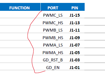
After analyzing with an oscilloscope I found that the SPI signals, and CS signal set in the TPP config block, they do not have the right shape (waveform) after the level shifter placed on the MPC board. I'm not sure about the cause but here is what you can do.
First, you must disable the outputs of the level shifter IC connected to SPI input signals of GD3000. By disabling its outputs we can then connect other SPI pins with wire jumpers to the same SPI inputs of GD3000.
So, to disable the outputs of this level shifter IC (U104) (placed on MPC5744P EVB) you must connect jumper J23. Now we must reroute other SPI signals to the same GD3000 inputs. I chose SPI 1 instance with pins: PA6 - SCK, PA7 - SOUT, and PA8 - SIN. Then I connected these pins with wire-jumpers to LT_PC5, LT_PC6, and LT_PC6. By disabling outputs of U104 we have disconnected the CS pin too, so I chose PTA3 to connect to LT_PE15.
I have updated your test1 project with what I told you here.
Best regards,
Adrian
- 新着としてマーク
- ブックマーク
- 購読
- ミュート
- RSS フィードを購読する
- ハイライト
- 印刷
- 不適切なコンテンツを報告
Hello,Adrian
I have connected the jumper 23 and SPI1 pins by wirejumpers.
But it still did not work. I found the LT_PA11 pin was kept zero.
After that I used the stateflow to configure the initialization sequence as the same SPI1 config.
The deadtime was still 15us.
It was so longtime.
Can you help me check it again by test2 as mentioned before?
Thank you very much
best regards
hao
- 新着としてマーク
- ブックマーク
- 購読
- ミュート
- RSS フィードを購読する
- ハイライト
- 印刷
- 不適切なコンテンツを報告
Hi @haoxue1027 ,
I checked the "test2" project, and the initialization of GD3000 it fails too, due to SPI level shifter (I think). So I recommend you to used TPP blocks and try to use other SPI instance, not the default one.
Have you tried a simple example using MBDT to check your setup ?
Is your power source delivering 12V and at least 1A ?
Best regards,
Adrian
- 新着としてマーク
- ブックマーク
- 購読
- ミュート
- RSS フィードを購読する
- ハイライト
- 印刷
- 不適切なコンテンツを報告
@adriantudor Hello,Adrian
Thank you for replying.
I am so sad to hear that test 2 was failed.but it can run in my board.just the deadtime was 15us.
I have try to use the SPI in the TPP blocks as you mentioned,but it still failed.
I have tested the demo of ADC,FLEXPWM, Etimer and so on , it was ok.
So I think the setup is ok. In addition ,the Power source can provide 24V/5A at most.
You have said that the SPI level shifter seemed not goodwork.
Does it means that there is a bug in the hardware or software?
Did you have any other recommends?
Thank you very much.
best regards
hao
- 新着としてマーク
- ブックマーク
- 購読
- ミュート
- RSS フィードを購読する
- ハイライト
- 印刷
- 不適切なコンテンツを報告
Hi @haoxue1027,
I hope that you have not connected your power source when it was set to 24V, because in that case, at least one o your boards can have some electronic components burned. The power source should be set to 12V and it's highly recommended to have overcurrent protection enabled and set to 1A at the beginning and after your setup and code is working properly you can increase overcurrent according to your needs.
It's a good thing that you could test a few demos.
My recommendation for you is to try your "test1" project with your jumper setup (using SPI0) and after the flashing process has been finished, create a power cycle(power off, wait a few seconds then power on both boards). Please let me know if that works for you.
Best regards,
Adrian
- 新着としてマーク
- ブックマーク
- 購読
- ミュート
- RSS フィードを購読する
- ハイライト
- 印刷
- 不適切なコンテンツを報告
@adriantudor Hello,adrian
I found there was a slight error in your proposed PIN connection(the location of PC5,6,7.).
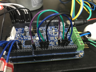
So I have tested again like following.
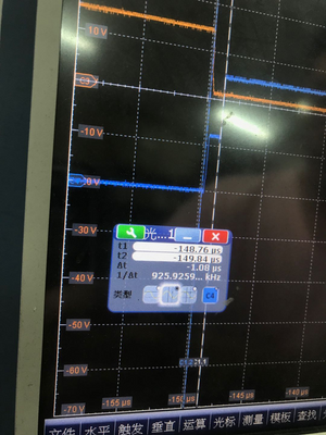
Fortunately, it worked as deadtime config(1000ns)!~~~A power cycle does not seem neccessary.
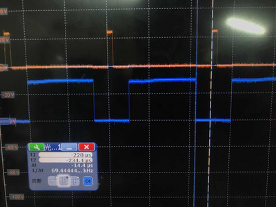
But there is a step in the PWM signal like following.
I want to confirm again, Is this normal ?
Thank you very much.
best regards
hao
- 新着としてマーク
- ブックマーク
- 購読
- ミュート
- RSS フィードを購読する
- ハイライト
- 印刷
- 不適切なコンテンツを報告
@haoxue1027 Hi Hao,
Please see my jumpers setup and if you want to try it (this one it's working with default pins and SPI0). I want to mention that this setup it's working for me but you have to remove 2 resistors from DEVKIT-MOTORGD : R70 and R73. The reason to remove those two resistors is that the output impedance of the level shifter it affect the signal if at the output is connected a pullup or pulldown resistor lower than 50kohm.
Your PWM output it's normal.
Best regards,
Adrian
- 新着としてマーク
- ブックマーク
- 購読
- ミュート
- RSS フィードを購読する
- ハイライト
- 印刷
- 不適切なコンテンツを報告
@adriantudor hello,Adrian
I will try to default pin and SPI0 later.
Thank you for helping me to solve this problem.
best regards
hao
