- Forums
- Product Forums
- General Purpose MicrocontrollersGeneral Purpose Microcontrollers
- i.MX Forumsi.MX Forums
- QorIQ Processing PlatformsQorIQ Processing Platforms
- Identification and SecurityIdentification and Security
- Power ManagementPower Management
- MCX Microcontrollers
- S32G
- S32K
- S32V
- MPC5xxx
- Other NXP Products
- Wireless Connectivity
- S12 / MagniV Microcontrollers
- Powertrain and Electrification Analog Drivers
- Sensors
- Vybrid Processors
- Digital Signal Controllers
- 8-bit Microcontrollers
- ColdFire/68K Microcontrollers and Processors
- PowerQUICC Processors
- OSBDM and TBDML
- S32M
-
- Solution Forums
- Software Forums
- MCUXpresso Software and ToolsMCUXpresso Software and Tools
- CodeWarriorCodeWarrior
- MQX Software SolutionsMQX Software Solutions
- Model-Based Design Toolbox (MBDT)Model-Based Design Toolbox (MBDT)
- FreeMASTER
- eIQ Machine Learning Software
- Embedded Software and Tools Clinic
- S32 SDK
- S32 Design Studio
- GUI Guider
- Zephyr Project
- Voice Technology
- Application Software Packs
- Secure Provisioning SDK (SPSDK)
- Processor Expert Software
-
- Topics
- Mobile Robotics - Drones and RoversMobile Robotics - Drones and Rovers
- NXP Training ContentNXP Training Content
- University ProgramsUniversity Programs
- Rapid IoT
- NXP Designs
- SafeAssure-Community
- OSS Security & Maintenance
- Using Our Community
-
- Cloud Lab Forums
-
- Knowledge Bases
- ARM Microcontrollers
- i.MX Processors
- Identification and Security
- Model-Based Design Toolbox (MBDT)
- QorIQ Processing Platforms
- S32 Automotive Processing Platform
- Wireless Connectivity
- CodeWarrior
- MCUXpresso Suite of Software and Tools
- MQX Software Solutions
-
MPC5746C LINFlexD_1 DMARXE DMATXE
Hi,
I am having a similar problem as this post.
IVOR 1 when writing to LINFlex DMATXE
DMA Mode on LIN0 works fine.
I tried doing what the post suggested, but it's not working for me.
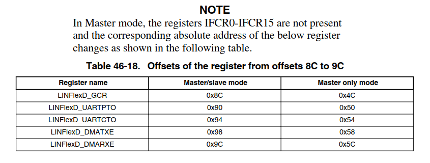
I don't see the offset table in the RM.
LINFlexD_1.UARTCR.R = 1; // set the UART bit first to be able to write the other bits
LINFlexD_1.UARTCR.B.WL1 = 0; // 8 bits data when PCE = 0 or 8 bits data + parity when PCE = 1
LINFlexD_1.UARTCR.B.WL0 = 1; // 8 bits data when PCE = 0 or 8 bits data + parity when PCE = 1
LINFlexD_1.UARTCR.B.TxEn = 1; // Transmitter Enabled
LINFlexD_1.UARTCR.B.RxEn = 1; // Receiver Enabled
LINFlexD_1.UARTCR.B.RFBM = 1; // UART Rx FIFO Mode Enabled (DMA requirement)
LINFlexD_1.UARTCR.B.TFBM = 1; // UART Tx FIFO Mode Enabled (DMA requirement)
//LINFlexD_1.DMARXE.R = 0x0000ffff; // Enable DMA //see https://community.nxp.com/thread/463696
//LINFlexD_1.DMATXE.R = 0x0000ffff; // Enable DMA //see https://community.nxp.com/thread/463696
//(*(vuint32_t *) (0xFBE8C000UL + (32 * 23)) ) = 0x0000FFFFUL;
//(*(vuint32_t *) (0xFBE8C000UL + (32 * 24)) ) = 0x0000FFFFUL;
//LINFlexD_1.IFCR[3].R = 0x0000ffff; // Enable DMA //see https://community.nxp.com/thread/463696
//LINFlexD_1.IFCR[4].R = 0x0000ffff; // Enable DMA //see https://community.nxp.com/thread/463696
LINFlexD_1.LINIER.B.DRIE = 0; // Disable RX Interrupt (DMA requirement)
LINFlexD_1.LINIER.B.DTIE = 0; // Disable Tx Interrupt (DMA requirement)
Hi,
offsets are mentioned in module's Memory map and register description chapter 46.5, see Table 46-18
following instruction should work
(*(vuint32_t *) (0xFBE8C000UL + (0x58)) ) = 0x1; // Enable DMA TX
(*(vuint32_t *) (0xFBE8C000UL + (0x5C)) ) = 0x1; // Enable DMA RX
Below lines should work too, depends on header file
LINFlexD_1.IFCR[3].R = 0x1; // Enable DMA TX
LINFlexD_1.IFCR[4].R = 0x1; // Enable DMA RX
Note: there are just 2 DMA request per module, so only lowest bit are implemented.
BR, Petr
