- Forums
- Product Forums
- General Purpose MicrocontrollersGeneral Purpose Microcontrollers
- i.MX Forumsi.MX Forums
- QorIQ Processing PlatformsQorIQ Processing Platforms
- Identification and SecurityIdentification and Security
- Power ManagementPower Management
- Wireless ConnectivityWireless Connectivity
- RFID / NFCRFID / NFC
- MCX Microcontrollers
- S32G
- S32K
- S32V
- MPC5xxx
- Other NXP Products
- S12 / MagniV Microcontrollers
- Powertrain and Electrification Analog Drivers
- Sensors
- Vybrid Processors
- Digital Signal Controllers
- 8-bit Microcontrollers
- ColdFire/68K Microcontrollers and Processors
- PowerQUICC Processors
- OSBDM and TBDML
- S32M
-
- Solution Forums
- Software Forums
- MCUXpresso Software and ToolsMCUXpresso Software and Tools
- CodeWarriorCodeWarrior
- MQX Software SolutionsMQX Software Solutions
- Model-Based Design Toolbox (MBDT)Model-Based Design Toolbox (MBDT)
- FreeMASTER
- eIQ Machine Learning Software
- Embedded Software and Tools Clinic
- S32 SDK
- S32 Design Studio
- GUI Guider
- Zephyr Project
- Voice Technology
- Application Software Packs
- Secure Provisioning SDK (SPSDK)
- Processor Expert Software
-
- Topics
- Mobile Robotics - Drones and RoversMobile Robotics - Drones and Rovers
- NXP Training ContentNXP Training Content
- University ProgramsUniversity Programs
- Rapid IoT
- NXP Designs
- SafeAssure-Community
- OSS Security & Maintenance
- Using Our Community
-
- Cloud Lab Forums
-
- Knowledge Bases
- ARM Microcontrollers
- i.MX Processors
- Identification and Security
- Model-Based Design Toolbox (MBDT)
- QorIQ Processing Platforms
- S32 Automotive Processing Platform
- Wireless Connectivity
- CodeWarrior
- MCUXpresso Suite of Software and Tools
- MQX Software Solutions
-
- RSS フィードを購読する
- トピックを新着としてマーク
- トピックを既読としてマーク
- このトピックを現在のユーザーにフロートします
- ブックマーク
- 購読
- ミュート
- 印刷用ページ
- 新着としてマーク
- ブックマーク
- 購読
- ミュート
- RSS フィードを購読する
- ハイライト
- 印刷
- 不適切なコンテンツを報告
When testing the RAM data bus, a popular solution is the "walking-1's" test. There are several patterns read from ROM, written then in a RAM address, and then read-back. However, there is no mention of the interference of the data cache. Since when we first read the pattern from the ROM, that pattern has to be stored in the data cache. When doing the read-back operation, the processor can optimize this operation by sending the pattern from the data cache, rather then the one from the RAM address, because no modification has been done to the pattern.
For the MPC5605B is there any way to "bypass" the data cache ? Like a data cache flush or inhibition ?
Also, if instead of a predefined pattern, we calculate the value by performing shift operations, will the data cache still interfere ?
解決済! 解決策の投稿を見る。
- 新着としてマーク
- ブックマーク
- 購読
- ミュート
- RSS フィードを購読する
- ハイライト
- 印刷
- 不適切なコンテンツを報告
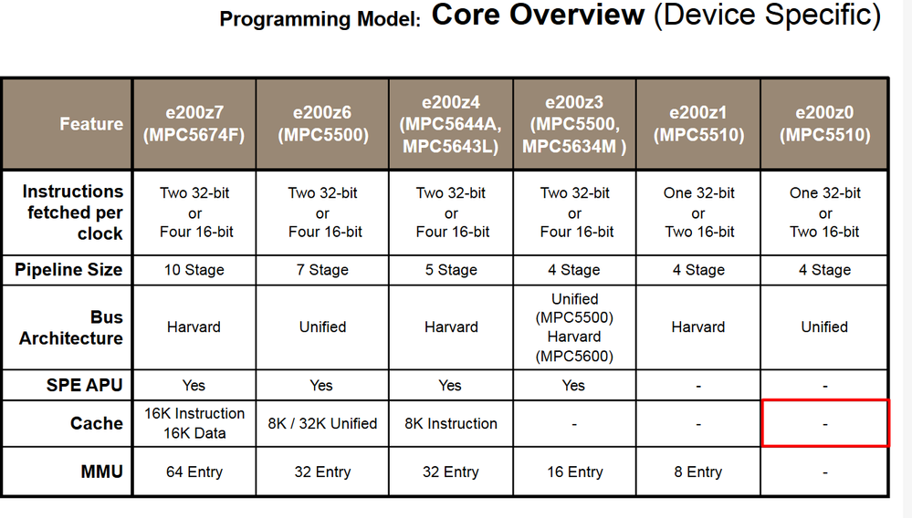
I have just realized you are using MPC5605B device, thus my previous answer is actually wrong because this device uses e200z0 core and it does not have cache nor MMU:
- 新着としてマーク
- ブックマーク
- 購読
- ミュート
- RSS フィードを購読する
- ハイライト
- 印刷
- 不適切なコンテンツを報告
I have just realized you are using MPC5605B device, thus my previous answer is actually wrong because this device uses e200z0 core and it does not have cache nor MMU:
- 新着としてマーク
- ブックマーク
- 購読
- ミュート
- RSS フィードを購読する
- ハイライト
- 印刷
- 不適切なコンテンツを報告
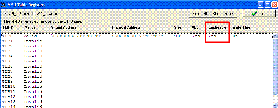
Hi, the portion of SRAM you want to test is needed to set for cache inhibited attribute i.e. to set up particular TLB entry in the MMU table. You may use following utility for simplifying of TLB configuration:
MMU Assist Register CONFIGURATOR
Note that every debugger or most of debuggers will be able to show MMU table in the screen like this:
Also I would like to point out following presentation, page 89-107:
e200 Core Training relevant to MPC55xx and MPC56xx device family
Note that if you have already stored some data and you are using copy-back mode, it may be necessary to invalidate the flash content.
You could also see following example code, file Optimizations.c, you may see there how to invalidate cache and also how to MMU attribute from cacheable to cache inhibited (but I must note it has been written for different device, so it may be slightly different):

