- Forums
- Product Forums
- General Purpose MicrocontrollersGeneral Purpose Microcontrollers
- i.MX Forumsi.MX Forums
- QorIQ Processing PlatformsQorIQ Processing Platforms
- Identification and SecurityIdentification and Security
- Power ManagementPower Management
- MCX Microcontrollers
- S32G
- S32K
- S32V
- MPC5xxx
- Other NXP Products
- Wireless Connectivity
- S12 / MagniV Microcontrollers
- Powertrain and Electrification Analog Drivers
- Sensors
- Vybrid Processors
- Digital Signal Controllers
- 8-bit Microcontrollers
- ColdFire/68K Microcontrollers and Processors
- PowerQUICC Processors
- OSBDM and TBDML
- S32M
-
- Solution Forums
- Software Forums
- MCUXpresso Software and ToolsMCUXpresso Software and Tools
- CodeWarriorCodeWarrior
- MQX Software SolutionsMQX Software Solutions
- Model-Based Design Toolbox (MBDT)Model-Based Design Toolbox (MBDT)
- FreeMASTER
- eIQ Machine Learning Software
- Embedded Software and Tools Clinic
- S32 SDK
- S32 Design Studio
- GUI Guider
- Zephyr Project
- Voice Technology
- Application Software Packs
- Secure Provisioning SDK (SPSDK)
- Processor Expert Software
-
- Topics
- Mobile Robotics - Drones and RoversMobile Robotics - Drones and Rovers
- NXP Training ContentNXP Training Content
- University ProgramsUniversity Programs
- Rapid IoT
- NXP Designs
- SafeAssure-Community
- OSS Security & Maintenance
- Using Our Community
-
- Cloud Lab Forums
-
- Knowledge Bases
- ARM Microcontrollers
- i.MX Processors
- Identification and Security
- Model-Based Design Toolbox (MBDT)
- QorIQ Processing Platforms
- S32 Automotive Processing Platform
- Wireless Connectivity
- CodeWarrior
- MCUXpresso Suite of Software and Tools
- MQX Software Solutions
-
- Home
- :
- Product Forums
- :
- MPC5xxx
- :
- Re: FLASH B erase error MPC5676
FLASH B erase error MPC5676
- Subscribe to RSS Feed
- Mark Topic as New
- Mark Topic as Read
- Float this Topic for Current User
- Bookmark
- Subscribe
- Mute
- Printer Friendly Page
- Mark as New
- Bookmark
- Subscribe
- Mute
- Subscribe to RSS Feed
- Permalink
- Report Inappropriate Content
hi,
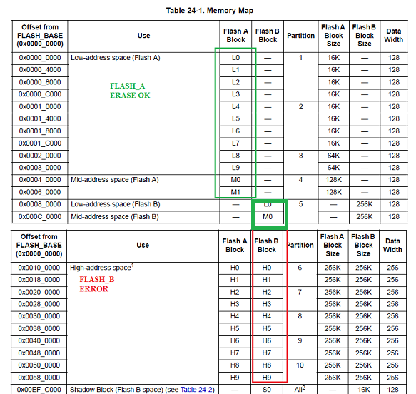
I have problems with Erase block B flash MPC5676.
Block A erase ok, L0~L9, M1~M0 and L0/M0 < update help
//----------------code test FLASH_B
DCACHE_Disable(); withh/winout
FLASH_B.HLR.R = 0xB2B22222; //password
FLASH_B.HLR.B.HBLOCK = 0x00 ; //unlock all blocks in high address space
//Erase
FLASH_B.MCR.B.ERS = 1;
FLASH_B.HSR.B.HBSEL = 0x01; // blocks H0
*(unsigned int *) 0x100000 = 0xFFFFFFFF;
FLASH_B.MCR.B.EHV = 1;
while ((FLASH_B.MCR.B.DONE == 0));
FLASH_B.MCR.B.EHV = 0;
FLASH_B.MCR.B.ERS = 0;
peg = FLASH_A.MCR.B.PEG;
//-------------------------updating it help
thanks,
Carlos.
Solved! Go to Solution.
- Mark as New
- Bookmark
- Subscribe
- Mute
- Subscribe to RSS Feed
- Permalink
- Report Inappropriate Content
Hi Carlos,
the flash is interleaved in high address space:
This helps to improve the performance. In case of non-interleaved flash, two physical reads of flash arrays are needed to fill one cache line. If the flash is interleaved, the blocks are read in parallel, so it looks like only one physical read is necessary.
The interlock write to 0x10_0000 falls to flash block A. So, it does not work as you can see. You need to write to 0x10_0000+16.
Or you can use SSD flash drivers which handle everything on background and you use the flash as linear address space. You do not need to care about blocks A and B ever:
https://www.nxp.com/lgfiles/Qorivva/MPC5674F_C90FL_SSD_DRV.exe
Regards,
Lukas
- Mark as New
- Bookmark
- Subscribe
- Mute
- Subscribe to RSS Feed
- Permalink
- Report Inappropriate Content
hi Lukas,
my code in RAM without ISR and exceptions_table,
so I chose the way to work with interlock.
write flash control address no problem, no near code have,
Erase high-address all space.
have solution do withot SSD driver ?
my test SSD : VLE_ON, COPYRAM_FALSE
ret = pFlashInit( &ssdConfig ); call not return
thanks,
Carlos
- Mark as New
- Bookmark
- Subscribe
- Mute
- Subscribe to RSS Feed
- Permalink
- Report Inappropriate Content
As I mentioned, there's no problem with your code. The interlock write just must fall within block B, that means you need to write to 0x10_0010, not to 0x10_0000.
Regarding SSD driver - I would need to see your code.
Regards,
Lukas
- Mark as New
- Bookmark
- Subscribe
- Mute
- Subscribe to RSS Feed
- Permalink
- Report Inappropriate Content
hi Lukas,
SSD solved problems,
thanks,
Carlos.

