- Forums
- Product Forums
- General Purpose MicrocontrollersGeneral Purpose Microcontrollers
- i.MX Forumsi.MX Forums
- QorIQ Processing PlatformsQorIQ Processing Platforms
- Identification and SecurityIdentification and Security
- Power ManagementPower Management
- MCX Microcontrollers
- S32G
- S32K
- S32V
- MPC5xxx
- Other NXP Products
- Wireless Connectivity
- S12 / MagniV Microcontrollers
- Powertrain and Electrification Analog Drivers
- Sensors
- Vybrid Processors
- Digital Signal Controllers
- 8-bit Microcontrollers
- ColdFire/68K Microcontrollers and Processors
- PowerQUICC Processors
- OSBDM and TBDML
- S32M
-
- Solution Forums
- Software Forums
- MCUXpresso Software and ToolsMCUXpresso Software and Tools
- CodeWarriorCodeWarrior
- MQX Software SolutionsMQX Software Solutions
- Model-Based Design Toolbox (MBDT)Model-Based Design Toolbox (MBDT)
- FreeMASTER
- eIQ Machine Learning Software
- Embedded Software and Tools Clinic
- S32 SDK
- S32 Design Studio
- GUI Guider
- Zephyr Project
- Voice Technology
- Application Software Packs
- Secure Provisioning SDK (SPSDK)
- Processor Expert Software
- MCUXpresso Training Hub
-
- Topics
- Mobile Robotics - Drones and RoversMobile Robotics - Drones and Rovers
- NXP Training ContentNXP Training Content
- University ProgramsUniversity Programs
- Rapid IoT
- NXP Designs
- SafeAssure-Community
- OSS Security & Maintenance
- Using Our Community
-
- Cloud Lab Forums
-
- Knowledge Bases
- ARM Microcontrollers
- i.MX Processors
- Identification and Security
- Model-Based Design Toolbox (MBDT)
- QorIQ Processing Platforms
- S32 Automotive Processing Platform
- Wireless Connectivity
- CodeWarrior
- MCUXpresso Suite of Software and Tools
- MQX Software Solutions
-
- Home
- :
- Product Forums
- :
- MPC5xxx
- :
- Re: EBI bus interface in MPC5777C controller
EBI bus interface in MPC5777C controller
- Subscribe to RSS Feed
- Mark Topic as New
- Mark Topic as Read
- Float this Topic for Current User
- Bookmark
- Subscribe
- Mute
- Printer Friendly Page
EBI bus interface in MPC5777C controller
- Mark as New
- Bookmark
- Subscribe
- Mute
- Subscribe to RSS Feed
- Permalink
- Report Inappropriate Content
Hi,
I have confusion on how to configure the data and address lines in EBI of MPC5777C controller.
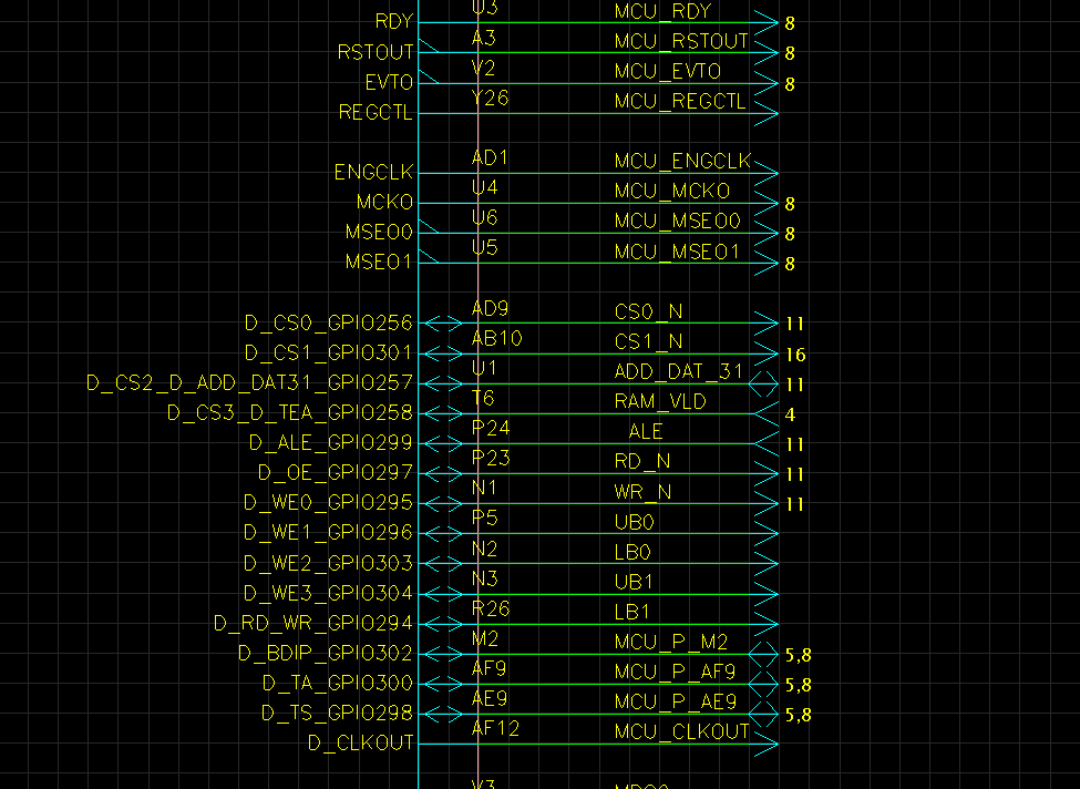
I want to use Muxed-32 bit mode (with two 1Mx16 MRAM chips (20 address lines) and two 64Mx16 NOR Flash chips) with chip selects 0 and 1 for MRAM and NOR flash respectively.
As shown in the table above, Address [9:15] are dedicated address pins and functionality will always be address irrespective of mode settings.
D_ADD_DAT[0:15] pins are multiplexed for Add#ress[0:15] and Data[0:15].
First of all, in pin-out of the controller, this name is not mentioned on these pins and it is mentioned as D_DAT[0:15].
1. Are these pins really multiplexed? or only function is data?
2. If they are multiplexed with Address[0:15], then Address[9:15] is getting duplicated at two places.
Will it be generated at two set of pins?
3. Address[9:15] can also be configured as GPIOs.
If I do so, will address duplication affect the function of my GPIOs, in case answer to question 2 is yes?
Also,
how pins D_OE, D_WE0, D_WE1, D_WE2, D_WE3, D_RD_WR are supposed to be used for different chip selects?
Thanks,
Shalaka
- Mark as New
- Bookmark
- Subscribe
- Mute
- Subscribe to RSS Feed
- Permalink
- Report Inappropriate Content
I already use this configuration with 32-bit bus and it works.
It work not on burst mode in my board
- Mark as New
- Bookmark
- Subscribe
- Mute
- Subscribe to RSS Feed
- Permalink
- Report Inappropriate Content
1) Yes, it is marked confused way but these pins can works as D_ADD_DAT[0:15] in multiplexed mode. I will suggest documentation improvement.
2) These are duplicated but D_ADD[9:15] contains only address thus they may not be buffered.
3) Yes, you can use these pins as GPIO if you don’t need it for EBI purpose.
4) D_OE, D_WE0, D_WE1, D_WE2, D_WE3, D_RD_WR will be shared for all devices connected (if all used, flash memories typically don’t need all WE lines). Only CS lines distinguish between connected device.
- Mark as New
- Bookmark
- Subscribe
- Mute
- Subscribe to RSS Feed
- Permalink
- Report Inappropriate Content
Thanks David.
I have one more question on this:
In 32-bit muxed mode, will ADD[9:15] be dedicated address lines? Will the address be valid throughout the write or read cycle?
I am basically latching only ADD_DAT[16:31] signals and connecting ADD[9:15] directly to memory to avoid using another latch for ADD_DAT[0:15] signals.
Will this work?
Thanks,
Shalaka
- Mark as New
- Bookmark
- Subscribe
- Mute
- Subscribe to RSS Feed
- Permalink
- Report Inappropriate Content
Yes, it is correct.
- Mark as New
- Bookmark
- Subscribe
- Mute
- Subscribe to RSS Feed
- Permalink
- Report Inappropriate Content
Thank you for the confirmation.


