- Forums
- Product Forums
- General Purpose MicrocontrollersGeneral Purpose Microcontrollers
- i.MX Forumsi.MX Forums
- QorIQ Processing PlatformsQorIQ Processing Platforms
- Identification and SecurityIdentification and Security
- Power ManagementPower Management
- Wireless ConnectivityWireless Connectivity
- RFID / NFCRFID / NFC
- Advanced AnalogAdvanced Analog
- MCX Microcontrollers
- S32G
- S32K
- S32V
- MPC5xxx
- Other NXP Products
- S12 / MagniV Microcontrollers
- Powertrain and Electrification Analog Drivers
- Sensors
- Vybrid Processors
- Digital Signal Controllers
- 8-bit Microcontrollers
- ColdFire/68K Microcontrollers and Processors
- PowerQUICC Processors
- OSBDM and TBDML
- S32M
- S32Z/E
-
- Solution Forums
- Software Forums
- MCUXpresso Software and ToolsMCUXpresso Software and Tools
- CodeWarriorCodeWarrior
- MQX Software SolutionsMQX Software Solutions
- Model-Based Design Toolbox (MBDT)Model-Based Design Toolbox (MBDT)
- FreeMASTER
- eIQ Machine Learning Software
- Embedded Software and Tools Clinic
- S32 SDK
- S32 Design Studio
- GUI Guider
- Zephyr Project
- Voice Technology
- Application Software Packs
- Secure Provisioning SDK (SPSDK)
- Processor Expert Software
- Generative AI & LLMs
-
- Topics
- Mobile Robotics - Drones and RoversMobile Robotics - Drones and Rovers
- NXP Training ContentNXP Training Content
- University ProgramsUniversity Programs
- Rapid IoT
- NXP Designs
- SafeAssure-Community
- OSS Security & Maintenance
- Using Our Community
-
- Cloud Lab Forums
-
- Knowledge Bases
- ARM Microcontrollers
- i.MX Processors
- Identification and Security
- Model-Based Design Toolbox (MBDT)
- QorIQ Processing Platforms
- S32 Automotive Processing Platform
- Wireless Connectivity
- CodeWarrior
- MCUXpresso Suite of Software and Tools
- MQX Software Solutions
- RFID / NFC
- Advanced Analog
-
- NXP Tech Blogs
- Home
- :
- MCUXpresso Software and Tools
- :
- MCUXpresso IDE
- :
- Running and debugging program in SDRAM
Running and debugging program in SDRAM
- Subscribe to RSS Feed
- Mark Topic as New
- Mark Topic as Read
- Float this Topic for Current User
- Bookmark
- Subscribe
- Mute
- Printer Friendly Page
Running and debugging program in SDRAM
- Mark as New
- Bookmark
- Subscribe
- Mute
- Subscribe to RSS Feed
- Permalink
- Report Inappropriate Content
Hi everyone,
I'm using a MIMXRT1024-EVK board, MCUXpresso 11.5.0 and SDK 2.11.0.
I'm trying to use this device in various cases, I've successfully compiled and debugged a project running both in flash and internal ram.
Now I'm trying to do the same thing in external SDRAM, but with no success.
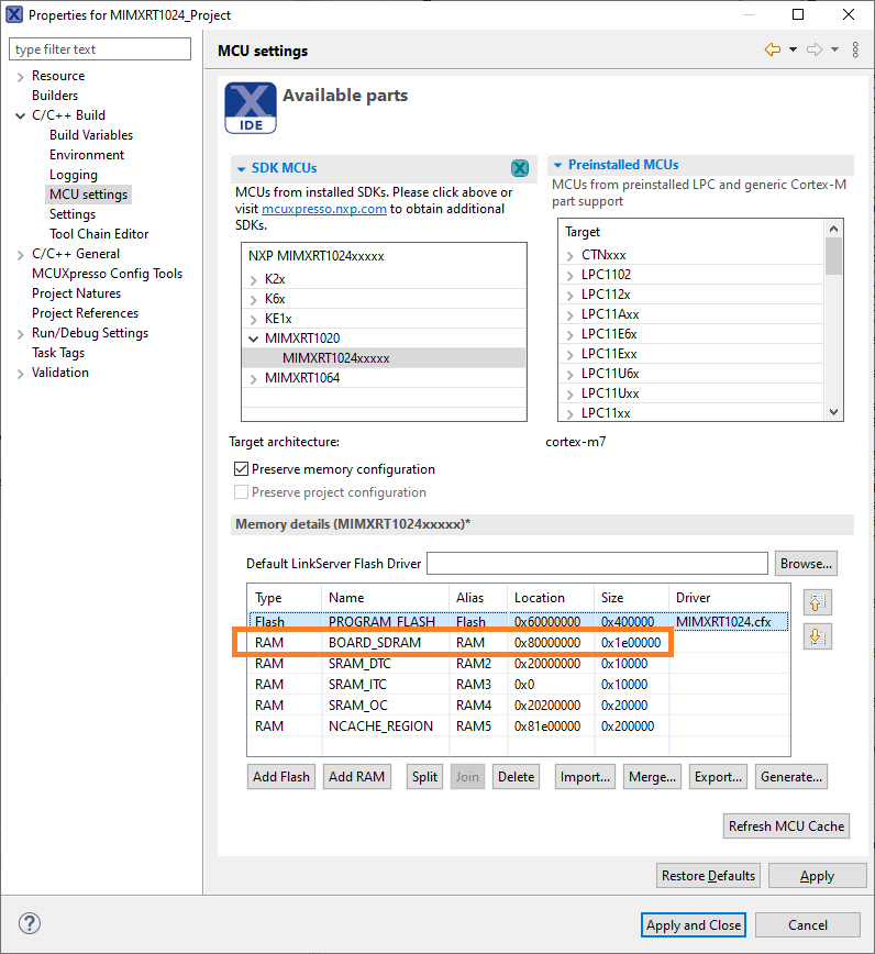
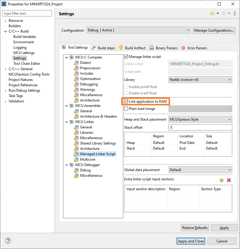
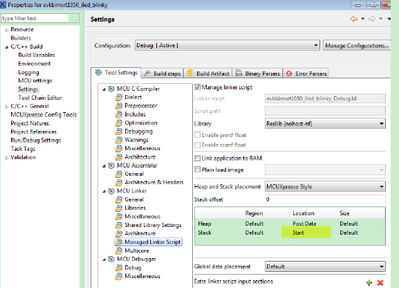
I've modified the project settings:
The project is correctly built and linked to SDRAM:
Memory region         Used Size  Region Size  %age Used
   PROGRAM_FLASH:          0 GB         4 MB      0.00%
     BOARD_SDRAM:       51496 B        30 MB      0.16%
        SRAM_DTC:          0 GB        64 KB      0.00%
        SRAM_ITC:          0 GB        64 KB      0.00%
         SRAM_OC:          0 GB       128 KB      0.00%
   NCACHE_REGION:          0 GB         2 MB      0.00%
.text 0x80000000 0x7bec
FILL mask 0xff
0x80000000 __vectors_start__ = ABSOLUTE (.)
*(SORT_BY_ALIGNMENT(.isr_vector))
.isr_vector 0x80000000 0x278 ./startup/startup_mimxrt1024.o
0x80000000 g_pfnVectors
0x80000000 __Vectors
0x80000278 . = ALIGN (0x4)
0x80000278 __section_table_start = .
0x80000278 __data_section_table = .
0x80000278 0x4 LONG 0x80007bec LOADADDR (.data)
0x8000027c 0x4 LONG 0x80007bec ADDR (.data)
0x80000280 0x4 LONG 0x118 SIZEOF (.data)
0x80000284 0x4 LONG 0x80007bec LOADADDR (.data_RAM2)
0x80000288 0x4 LONG 0x20000000 ADDR (.data_RAM2)
0x8000028c 0x4 LONG 0x0 SIZEOF (.data_RAM2)
0x80000290 0x4 LONG 0x80007bec LOADADDR (.data_RAM3)
0x80000294 0x4 LONG 0x0 ADDR (.data_RAM3)
0x80000298 0x4 LONG 0x0 SIZEOF (.data_RAM3)
0x8000029c 0x4 LONG 0x80007bec LOADADDR (.data_RAM4)
0x800002a0 0x4 LONG 0x20200000 ADDR (.data_RAM4)
0x800002a4 0x4 LONG 0x0 SIZEOF (.data_RAM4)
0x800002a8 0x4 LONG 0x80007bec LOADADDR (.data_RAM5)
0x800002ac 0x4 LONG 0x81e00000 ADDR (.data_RAM5)
0x800002b0 0x4 LONG 0x0 SIZEOF (.data_RAM5)
0x800002b4 __data_section_table_end = .
0x800002b4 __bss_section_table = .
0x800002b4 0x4 LONG 0x80007d04 ADDR (.bss)
0x800002b8 0x4 LONG 0x2c24 SIZEOF (.bss)
0x800002bc 0x4 LONG 0x20000000 ADDR (.bss_RAM2)
0x800002c0 0x4 LONG 0x0 SIZEOF (.bss_RAM2)
0x800002c4 0x4 LONG 0x0 ADDR (.bss_RAM3)
0x800002c8 0x4 LONG 0x0 SIZEOF (.bss_RAM3)
0x800002cc 0x4 LONG 0x20200000 ADDR (.bss_RAM4)
0x800002d0 0x4 LONG 0x0 SIZEOF (.bss_RAM4)
0x800002d4 0x4 LONG 0x81e00000 ADDR (.bss_RAM5)
0x800002d8 0x4 LONG 0x0 SIZEOF (.bss_RAM5)
0x800002dc __bss_section_table_end = .
0x800002dc __section_table_end = .
*(SORT_BY_ALIGNMENT(.after_vectors*))
.after_vectors.reset
0x800002dc 0x54 ./startup/startup_mimxrt1024.o
0x800002dc ResetISR
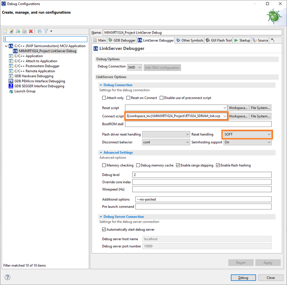
Based on this post, I've modified the lunch configuration settings:
The RT1024_SDRAM_Init.scp attached file is modified compared to RT1050_Debug_Connect.scp file referred in the post due to different registers addresses.
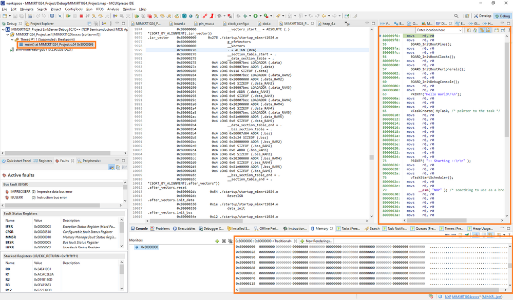
When I start to debug the project I can see that it refers to SDRAM (the current location is at 0x800005F6), but all the SDRAM content is 0 and I can't even modify it.
From the console debug messages it seems that the program isn't downloaded:
MCUXpresso IDE RedlinkMulti Driver v11.5 (Dec 16 2021 12:38:31 - crt_emu_cm_redlink build 2)
Found chip XML file in C:/Users/francesco/Documents/MCUXpressoIDE_11.5.0_7232/workspace/MIMXRT1024_Project/Debug\MIMXRT1024xxxxx.xml
(  5) Remote configuration complete
Reconnected to existing LinkServer process.
============= SCRIPT: C:\Users\francesco\Documents\MCUXpressoIDE_11.5.0_7232\workspace\MIMXRT1024_Project\RT1024_SDRAM_Init.scp =============
RT1024 SDRAM Initialisation
Clock Init Done
SDRAM Init Done
============= END SCRIPT ====================================================================================================================
Probe Firmware: CMSIS-DAP (ARM)
Serial Number:  02380000092c2cb500000000000000000000000097969905
VID:PID:  0D28:0204
USB Path: \\?\hid#vid_0d28&pid_0204&mi_03#7&38571b4c&0&0000#{4d1e55b2-f16f-11cf-88cb-001111000030}
Using memory from core 0 after searching for a good core
debug interface type      = CoreSight DP (DAP DP ID 0BD11477) over SWD TAP 0
processor type            = Cortex-M7 (CPU ID 00000C27) on DAP AP 0
number of h/w breakpoints = 8
number of flash patches   = 0
number of h/w watchpoints = 4
Probe(0): Connected&Reset. DpID: 0BD11477. CpuID: 00000C27. Info: <None>
Debug protocol: SWD. RTCK: Disabled. Vector catch: Disabled.
Content of CoreSight Debug ROM(s):
RBASE E00FD000: CID B105100D PID 000008E88C ROM (type 0x1)
ROM 1 E00FE000: CID B105100D PID 04000BB4C8 ROM (type 0x1)
ROM 2 E00FF000: CID B105100D PID 04000BB4C7 ROM (type 0x1)
ROM 3 E000E000: CID B105E00D PID 04000BB00C Gen SCS (type 0x0)
ROM 3 E0001000: CID B105E00D PID 04000BB002 Gen DWT (type 0x0)
ROM 3 E0002000: CID B105E00D PID 04000BB00E Gen (type 0x0)
ROM 3 E0000000: CID B105E00D PID 04000BB001 Gen ITM (type 0x0)
ROM 2 E0041000: CID B105900D PID 04001BB975 CSt ARM ETMv4.0 type 0x13 Trace Source - Core
ROM 2 E0042000: CID B105900D PID 04004BB906 CSt type 0x14 Debug Control - Trigger, e.g. ECT
ROM 1 E0040000: CID B105900D PID 04000BB9A9 CSt type 0x11 Trace Sink - TPIU
ROM 1 E0043000: CID B105F00D PID 04001BB101 Sys (type 0x0)
NXP: MIMXRT1024xxxxx
DAP stride is 1024 bytes (256 words)
Connected: was_reset=false. was_stopped=true
Awaiting telnet connection to port 3330 ...
GDB nonstop mode disabled (using allstop mode)
FreeRTOS stack backtrace is enabled
Starting execution using soft reset with PC 0x0 SP 0x0 from load at 0x80000000
Stopped: Breakpoint #1
What am I missing to debug a program in SDRAM?
Many thanks
Biafra
- Mark as New
- Bookmark
- Subscribe
- Mute
- Subscribe to RSS Feed
- Permalink
- Report Inappropriate Content
Hi @kerryzhou,
Sorry for the delay, I was engaged in another activity.
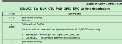
I've found the cause. In the RT1050_Debug_Connect.scp the configuration for the DQS pin is done using the SION bit (unlike all the other pins), setting the register value to 0x10.
In the RT1050 device the configuration register for the DQS pin is on the register IOMUXC_SW_MUX_CTL_PAD_GPIO_EMC_39 at the address 0x401F80B0.
In the RT1024 device the configuration register for the DQS pin is on the register IOMUXC_SW_MUX_CTL_PAD_GPIO_EMC_28 at the address 0x401F8084.
With the correct settings, I can debug fine in SDRAM.
Now this is my question: why is it needed to set the configuration register for the DQS to the value 0x10, unlike all the other SDRAM pins, for which the value 0x0 is used?
Many thanks
Biafra
- Mark as New
- Bookmark
- Subscribe
- Mute
- Subscribe to RSS Feed
- Permalink
- Report Inappropriate Content
Hi @biafra ,
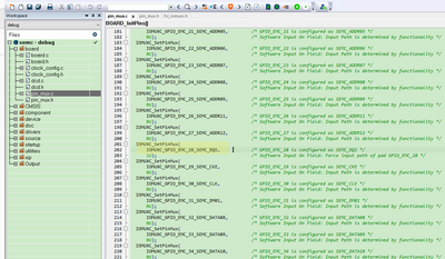
You mean this one:
IOMUXC_SetPinMux(
IOMUXC_GPIO_EMC_28_SEMC_DQS, /* GPIO_EMC_28 is configured as SEMC_DQS */
1U); /* Software Input On Field: Force input path of pad GPIO_EMC_28 */
static inline void IOMUXC_SetPinMux(uint32_t muxRegister,
uint32_t muxMode,
uint32_t inputRegister,
uint32_t inputDaisy,
uint32_t configRegister,
uint32_t inputOnfield)
{
*((volatile uint32_t *)muxRegister) =
IOMUXC_SW_MUX_CTL_PAD_MUX_MODE(muxMode) | IOMUXC_SW_MUX_CTL_PAD_SION(inputOnfield);
if (inputRegister != 0UL)
{
*((volatile uint32_t *)inputRegister) = inputDaisy;
}
}
The inputOnfield set as 1 in IOMUXC_SW_MUX_CTL_PAD_SION, right?
This will force input path of pad GPIO_EMC_28.
In fact, in the SDK code, it also set it.
Wish it helps you!
Best Regards,
Kerry
- Mark as New
- Bookmark
- Subscribe
- Mute
- Subscribe to RSS Feed
- Permalink
- Report Inappropriate Content
Hi @biafra
Please check these points:
1. XIP_BOOT_HEADER_DCD_ENABLE=1
2. stack location modify from end to start
Then test it again.
Please try it on your side.
If you still have issues about it, please kindly let me know.
Best Regards,
Kerry
