- Forums
- Product Forums
- General Purpose MicrocontrollersGeneral Purpose Microcontrollers
- i.MX Forumsi.MX Forums
- QorIQ Processing PlatformsQorIQ Processing Platforms
- Identification and SecurityIdentification and Security
- Power ManagementPower Management
- Wireless ConnectivityWireless Connectivity
- RFID / NFCRFID / NFC
- MCX Microcontrollers
- S32G
- S32K
- S32V
- MPC5xxx
- Other NXP Products
- S12 / MagniV Microcontrollers
- Powertrain and Electrification Analog Drivers
- Sensors
- Vybrid Processors
- Digital Signal Controllers
- 8-bit Microcontrollers
- ColdFire/68K Microcontrollers and Processors
- PowerQUICC Processors
- OSBDM and TBDML
- S32M
-
- Solution Forums
- Software Forums
- MCUXpresso Software and ToolsMCUXpresso Software and Tools
- CodeWarriorCodeWarrior
- MQX Software SolutionsMQX Software Solutions
- Model-Based Design Toolbox (MBDT)Model-Based Design Toolbox (MBDT)
- FreeMASTER
- eIQ Machine Learning Software
- Embedded Software and Tools Clinic
- S32 SDK
- S32 Design Studio
- GUI Guider
- Zephyr Project
- Voice Technology
- Application Software Packs
- Secure Provisioning SDK (SPSDK)
- Processor Expert Software
-
- Topics
- Mobile Robotics - Drones and RoversMobile Robotics - Drones and Rovers
- NXP Training ContentNXP Training Content
- University ProgramsUniversity Programs
- Rapid IoT
- NXP Designs
- SafeAssure-Community
- OSS Security & Maintenance
- Using Our Community
-
- Cloud Lab Forums
-
- Knowledge Bases
- ARM Microcontrollers
- i.MX Processors
- Identification and Security
- Model-Based Design Toolbox (MBDT)
- QorIQ Processing Platforms
- S32 Automotive Processing Platform
- Wireless Connectivity
- CodeWarrior
- MCUXpresso Suite of Software and Tools
- MQX Software Solutions
-
- Home
- :
- QorIQプロセッシングプラットフォーム
- :
- レイヤースケープ
- :
- Re: debug access to ddr_ctlr
debug access to ddr_ctlr
- RSS フィードを購読する
- トピックを新着としてマーク
- トピックを既読としてマーク
- このトピックを現在のユーザーにフロートします
- ブックマーク
- 購読
- ミュート
- 印刷用ページ
- 新着としてマーク
- ブックマーク
- 購読
- ミュート
- RSS フィードを購読する
- ハイライト
- 印刷
- 不適切なコンテンツを報告
Why can't we access the ddr controller without losing a JTAG connection?
Hi,
We're trying to bring up our custom board based on the LS1020a processor with DDR4 attached. I've used the QCVS tool to generate initialization code that I'm using in my bare-metal memory test app. I also use the generated register values in U-Boot. On the first access to the DDR controller registers, whether from my mem test app or from U-Boot, I lose my JTAG connection. In CCS and in CodeWarrior, I can see that CCS is reporting a "ScanTimeout". Do I have to do something special in order to access the DDR controller? Does anyone know of any situations that can cause this kind of behavior?
解決済! 解決策の投稿を見る。
- 新着としてマーク
- ブックマーク
- 購読
- ミュート
- RSS フィードを購読する
- ハイライト
- 印刷
- 不適切なコンテンツを報告
Thanks for all the help, Adrian. The problem is mostly resolved. I changed RCW1 and RCW6 (counting from 1) in flash to the values placed in the registers by the 0x9B hard-coded values. I could then connect (see caveat below). I then began adding my desired values back into the fields (in flash) one by one. After I enabled the DDR_REFCLK_SEL, I could see DDR registers! Hallelujah! If I couldn't connect without a hard-coded RCW after I changed a value, I would connect with the hard-coded RCW and restore that field to its working value. It seems like the mem_pll_rat and cga_pll_rat are giving me the most problems. If I set it up for a 1Ghz proc clock and a 800 Mhz DDR clock, then I can't connect via JTAG without the undesirable hard-coded RCW.
The caveat is that if you cycle power, the JTAG chain seems to get a grip on the proc. So a normal jtag attach with no RCW overrides will never free the proc and because the sequence doesn't do a "reset_to_debug". A connection with RCW overrides will free it, as will resetting to debug from CCS.
- 新着としてマーク
- ブックマーク
- 購読
- ミュート
- RSS フィードを購読する
- ハイライト
- 印刷
- 不適切なコンテンツを報告
Should be: (0x1000 0x80000001). Looks like ccs::config_template 0 2 0x80000001 is deprecate and ccs::config_template 0 4096 0x80000001 should be used.
Adrian
- 新着としてマーク
- ブックマーク
- 購読
- ミュート
- RSS フィードを購読する
- ハイライト
- 印刷
- 不適切なコンテンツを報告
yes, you need to use ccs::config_template 0 2 0x80000001 for fulll rcw override.
Adrian
- 新着としてマーク
- ブックマーク
- 購読
- ミュート
- RSS フィードを購読する
- ハイライト
- 印刷
- 不適切なコンテンツを報告
I thought that might be the case. How would one indicate that in the jtag config file? I changed (0x1000 1) to(2 0x80000001) but CCS then reports "Invalid Parameter".
- 新着としてマーク
- ブックマーク
- 購読
- ミュート
- RSS フィードを購読する
- ハイライト
- 印刷
- 不適切なコンテンツを報告
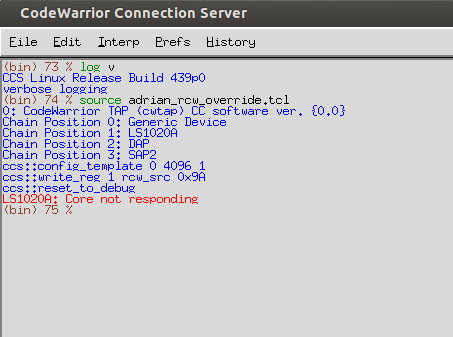
Did you also override the rcw regs? Is not visible in ccs console. Also, since reset to debug is not working and return Core not responding, my guess this is because the incorrect rcw.
Also, you can try with ccs::config_template 0 2 0x80000001; instead of ccs::config_template 0 4096 1; This way the rcw oveeride will include also the PLL.
Adrian
- 新着としてマーク
- ブックマーク
- 購読
- ミュート
- RSS フィードを購読する
- ハイライト
- 印刷
- 不適切なコンテンツを報告
I did update the RCWs with our values. I do suspect that our RCW5 value is causing problems as I posted earlier today. One thing about overriding the RCWs - I can never seem to connect, even on a previously working connection, if I try to override RCWs 1 through 5. Does that require a different RCW option than (0x1000 1)?
- 新着としてマーク
- ブックマーク
- 購読
- ミュート
- RSS フィードを購読する
- ハイライト
- 印刷
- 不適切なコンテンツを報告
I can now connect without using the hard-coded RCW. Still can't access the DDR controller registers, though. The key to this mini-breakthrough was changing 2 RCW values in QSPI flash. I changed them to the values used by the hard-coded RCW value 0x9A:
RCW | (desired values) | (working values) |
1 | 0x0608000A | 0x060A0006 |
6 | 0x08000020 | 0x00404000 |
I tried just changing one RCW or the other, but they were both needed. Perhaps it's not surprising that I still can't access DDR as that working RCW6 value doesn't configure a valid ref clock source for DDR on our board.
- 新着としてマーク
- ブックマーク
- 購読
- ミュート
- RSS フィードを購読する
- ハイライト
- 印刷
- 不適切なコンテンツを報告
- 新着としてマーク
- ブックマーク
- 購読
- ミュート
- RSS フィードを購読する
- ハイライト
- 印刷
- 不適切なコンテンツを報告
Hi Adrian,
Here is the output:
- 新着としてマーク
- ブックマーク
- 購読
- ミュート
- RSS フィードを購読する
- ハイライト
- 印刷
- 不適切なコンテンツを報告
Any advice on connecting to our board, without using the hard-coded RCW values in the JTAG ini file? I believe we are loading our RCWs from flash on RESET. The RCWs from the JTAG .ini and the RCWs in flash differ by only a few bits - particularly the rcw[DDR_REFCLK_SEL] field. When we try to connect without the hard-coded RCW, we most often get "core not responding"
We kind of suspect that the problem is that we're connecting via JTAG with the hard-coded RCW value 0x9A. It appears we are loading our RCW values from QSPI flash, but cannot seem to connect via JTAG in anyway unles we have the hard-coded RCW value set up in the JTAG ini file.
- 新着としてマーク
- ブックマーク
- 購読
- ミュート
- RSS フィードを購読する
- ハイライト
- 印刷
- 不適切なコンテンツを報告
We've done some more digging and found that all of the other components in the CCSR space seem to read back just fine. Even the reserved space right up to 0x0107FFF0. But the first read of 0x01080000 will cause a scan timeout. Is there anything that could cause the DDR controller to lock up such that it can't even respond to a JTAG read of its registers?
- 新着としてマーク
- ブックマーク
- 購読
- ミュート
- RSS フィードを購読する
- ハイライト
- 印刷
- 不適切なコンテンツを報告
Did the read works from ccs?
Adrian
- 新着としてマーク
- ブックマーク
- 購読
- ミュート
- RSS フィードを購読する
- ハイライト
- 印刷
- 不適切なコンテンツを報告
The reads do not work from CCS - scan_timeout. Some more info - we're connecting with the hard-coded RCW value 0x9A. Even though that's documented as selecting setting rcw[DDR_REFCLK_SEL] to 2, it actually sets it to 0 (Table 4-16 of the ARM). On the LS1021ATWR dev board, we've configured to boot from QSPI and erased QSPI so that its similar to our custom board. Connecting to the TWR with hard-coded RCW value 0x9B, we can still access the DDR registers. The critical difference might be that the TWR has a clock on the pin DDR_CLK, but our board doesn't. We are using SYS_CLK (differential) as the single source.
- 新着としてマーク
- ブックマーク
- 購読
- ミュート
- RSS フィードを購読する
- ハイライト
- 印刷
- 不適切なコンテンツを報告
Please check which particular physical address you are trying to access, if this address is valid (if this is a memory mapped register - please check it has valid offset), and how this memory space is configured in memory management unit.
Have a great day,
Alexander
-----------------------------------------------------------------------------------------------------------------------
Note: If this post answers your question, please click the Correct Answer button. Thank you!
-----------------------------------------------------------------------------------------------------------------------
- 新着としてマーク
- ブックマーク
- 購読
- ミュート
- RSS フィードを購読する
- ハイライト
- 印刷
- 不適切なコンテンツを報告
Hi Alexander,
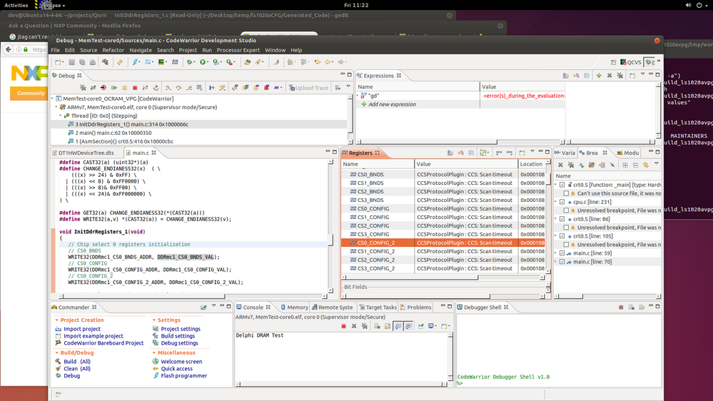
This is a straight read of a memory mapped DDR controller register. You can't quite see the full addresses in the picture I attached, but they match the datasheet addresses for the DDR controller i.e. 0x0108_0000
- 新着としてマーク
- ブックマーク
- 購読
- ミュート
- RSS フィードを購読する
- ハイライト
- 印刷
- 不適切なコンテンツを報告
Please make sure core is suspended. CW will do all accesses via core and if core is running, you will get "Scan timeout" message.
Adrian
- 新着としてマーク
- ブックマーク
- 購読
- ミュート
- RSS フィードを購読する
- ハイライト
- 印刷
- 不適切なコンテンツを報告
Hi Adrian,
It's not shown as suspended in the picture I attached, but the results are the same even when it is suspended.

