- Forums
- Product Forums
- General Purpose MicrocontrollersGeneral Purpose Microcontrollers
- i.MX Forumsi.MX Forums
- QorIQ Processing PlatformsQorIQ Processing Platforms
- Identification and SecurityIdentification and Security
- Power ManagementPower Management
- MCX Microcontrollers
- S32G
- S32K
- S32V
- MPC5xxx
- Other NXP Products
- Wireless Connectivity
- S12 / MagniV Microcontrollers
- Powertrain and Electrification Analog Drivers
- Sensors
- Vybrid Processors
- Digital Signal Controllers
- 8-bit Microcontrollers
- ColdFire/68K Microcontrollers and Processors
- PowerQUICC Processors
- OSBDM and TBDML
- S32M
-
- Solution Forums
- Software Forums
- MCUXpresso Software and ToolsMCUXpresso Software and Tools
- CodeWarriorCodeWarrior
- MQX Software SolutionsMQX Software Solutions
- Model-Based Design Toolbox (MBDT)Model-Based Design Toolbox (MBDT)
- FreeMASTER
- eIQ Machine Learning Software
- Embedded Software and Tools Clinic
- S32 SDK
- S32 Design Studio
- GUI Guider
- Zephyr Project
- Voice Technology
- Application Software Packs
- Secure Provisioning SDK (SPSDK)
- Processor Expert Software
- MCUXpresso Training Hub
-
- Topics
- Mobile Robotics - Drones and RoversMobile Robotics - Drones and Rovers
- NXP Training ContentNXP Training Content
- University ProgramsUniversity Programs
- Rapid IoT
- NXP Designs
- SafeAssure-Community
- OSS Security & Maintenance
- Using Our Community
-
- Cloud Lab Forums
-
- Knowledge Bases
- ARM Microcontrollers
- i.MX Processors
- Identification and Security
- Model-Based Design Toolbox (MBDT)
- QorIQ Processing Platforms
- S32 Automotive Processing Platform
- Wireless Connectivity
- CodeWarrior
- MCUXpresso Suite of Software and Tools
- MQX Software Solutions
-
- Home
- :
- QorIQ Processing Platforms
- :
- Layerscape
- :
- Re: HRe: LS1017 features Vs single core operations and security functions
LS1017 features Vs single core operations and security functions
- Subscribe to RSS Feed
- Mark Topic as New
- Mark Topic as Read
- Float this Topic for Current User
- Bookmark
- Subscribe
- Mute
- Printer Friendly Page
LS1017 features Vs single core operations and security functions
- Mark as New
- Bookmark
- Subscribe
- Mute
- Subscribe to RSS Feed
- Permalink
- Report Inappropriate Content
I would use the LS1017 for safety critical applications and therefore my questions are the following:
1) Is LS1017 a true single core? Since the LS1017 device is based on the LS1027 (Dual core), how the second core is implemented on the die? Is it removed, switched off or what else? Should the SW disable the second core?
2) Is the base P/N LS1017AXN7PQA with Security disabled, able to perform a secure boot? During the SoC's secure boot process the boot ROM code uses the Super Root Key Hash (SRKH) stored in the SoC's fuse bank to verify a public key that is then used to verify the signature over the device's boot image. So the boot ROM code is trusted. Can the device "LS1017AXN7PQA" use the secure boot function?
Thanks
Maurizio
- Mark as New
- Bookmark
- Subscribe
- Mute
- Subscribe to RSS Feed
- Permalink
- Report Inappropriate Content
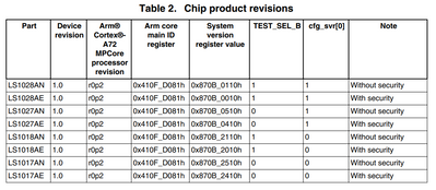
Therefore the LS1017 is a dual core with the second core physically disabled through the signals TEST_SEL_B and cfg_svr[0], however the reference manual and datasheet don’t clarify how to manage these signals. Could you please clarify if they should be connected to GND via pull-down and disabled via SW?
Furthermore, last but not least, if the above pins would not be connected to GND the LS1017 would work as a dual core like the LS1027. Do you confirm? If so what is the difference to buy the LS1017 instead of LS1027? Please consider this confirmation very important.
Thanks
Maurizio1
- Mark as New
- Bookmark
- Subscribe
- Mute
- Subscribe to RSS Feed
- Permalink
- Report Inappropriate Content
Hi @Maurizio1!
Thank you for contacting NXP Support!
Q1, the second core is physically disabled. Refer to Table 2 of the LS1028A Design Checklist "AN12028". It shows the pins selection for the different product versions (TEST_SEL_B and cfg_svr[0])
Q2) LS1017AXN7PQA part number, none of the security functions are enabled including the secureboot.
Best Regards.
Chavira
- Mark as New
- Bookmark
- Subscribe
- Mute
- Subscribe to RSS Feed
- Permalink
- Report Inappropriate Content
Sorry, but your last answer doesn't provide a reply for this question: if the above pins would not be connected to GND the LS1017 would work as a dual core like the LS1027. Do you confirm? If so what is the difference to buy/use the LS1017 instead of LS1027? Please consider this confirmation very important.
Could you please answer to this question, because in safety application is not recommended to have a second core which could suddenly switched on.
Many thanks for your cooperation.
Best Regards
Maurizio
- Mark as New
- Bookmark
- Subscribe
- Mute
- Subscribe to RSS Feed
- Permalink
- Report Inappropriate Content
Hi @Maurizio1!
No, the LS1017A has the second core disabled for hardware in the silicon, you shouldn't disable it for Software because is not connected physically.
I am waiting for the internal team to confirm the pin termination on LS1017, I think is not important for those pins on LS1017 because those pins are only for LS1027 and LS1028.
Best Regards.
Chavira
- Mark as New
- Bookmark
- Subscribe
- Mute
- Subscribe to RSS Feed
- Permalink
- Report Inappropriate Content
Hi Chavira,
many thanks for yuor reply. Therefore summarizing the second core is HW physically not connected, but the pins should be connected to GND as in table of AN12028. However the pin cfg_svr[0] has more functions and if it is not so important can we use it as XSPI1_A_CS0_B? Otherwise we lose the chip select on XSPI1 bus.
Thanks
Regards
Maurizio1
- Mark as New
- Bookmark
- Subscribe
- Mute
- Subscribe to RSS Feed
- Permalink
- Report Inappropriate Content
Hi @Maurizio1 !
The cfg_svr[0] ( i.e. all cfg type of pins) state is assessed at boot-up (i.e before PORESET is asserted). After PORESET is released, the cfg_svr[0] pin can be used accordingly to how the pin muxing is defined.
Refer to note 4 in from Table 1 of the LS1027A datasheet:
4. This pin is a reset configuration pin. It has a weak (~20 k ) internal pull-up P-FET that is enabled only when the processor is in its reset state. This pull-up is designed such that it can be overpowered by an external 4.7 k resistor. However, if the signal is intended to be high after reset, and if there is any device on the net that might pull down the value of the net at reset, a pull-up or active driver is needed.
- Mark as New
- Bookmark
- Subscribe
- Mute
- Subscribe to RSS Feed
- Permalink
- Report Inappropriate Content
Hi Chavira,
just to clarify the usefulness of these signals, could you please clarify why it is necessary to set the pin (TEST_SEL & CFG_SVR0) to 0 at boot-up if both second CORE and GPU are not physically connected?
If TEST_SEL & CFG_SVR0 weren't connected to 0 what happens? It is important to clarify this point because we need to be sure that both the second core and the GPU must not interfere with the active core.
Thanks
Maurizio1
- Mark as New
- Bookmark
- Subscribe
- Mute
- Subscribe to RSS Feed
- Permalink
- Report Inappropriate Content
Hi @Maurizio1!
Functionally, this pin is an output or an input, but structurally it is an I/O because it is either a sample configuration input during reset, is a muxed pin, or has other manufacturing test functions.
For LS1017A you have to follow the instructions of the datasheet, we don't have documentation about the behavior of the LS1017A in case of don't follow the datasheet, you can expect random failures.
You can put those pins like LS1027A or LS1028A but the LS1017A never will have the behavior of the LS1027A because doesn't have the same hardware.
If you have the LS1017A you can be sure of the second core or the GPU is not connected and you don't have to configure or disable anything.
- Mark as New
- Bookmark
- Subscribe
- Mute
- Subscribe to RSS Feed
- Permalink
- Report Inappropriate Content
Hi Chavira,
I understand that the documentation doesn't provide all answers, however you could ask help your designers to clarify better what is not written in the datasheet. The LS1017 is confirmed that has a different HW, but the signals TEST_SEL & CFG_SVR0 should be connected to 0 during reset time only. It seems that those signals serve either to read the chip product revision or switch-off something inside the chip at power-on. The doubt is still present if then they could cause some failures. I don't want to insist yet but for our application to settle the issue would be important.
Finally two questions: 1) Product longevity, do you know how many years is still available the product LS1017A? 2) The datasheet shows a block diagram with the on chip SRAM 256kB, while the reference manual removes the SRAM. What's the right block diagram?
Thanks for your cooperation.
- Mark as New
- Bookmark
- Subscribe
- Mute
- Subscribe to RSS Feed
- Permalink
- Report Inappropriate Content
Hi @Maurizio1 !
Those signals are important to prevent failures on the chip, please follow the datasheet and trust in our job, the second core and the GPU are not implemented on the LS1017A and you should configure nothing or disable manually the second core or the GPU because doesn't exist on LS1017A.
Q1) According to the Longevity program the LS1017A has support until 2033
Product Longevity | NXP Semiconductors
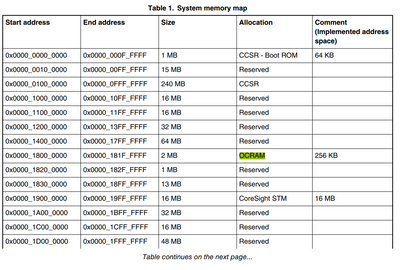
Q2) In the reference Manual you can find SRAM like OCRAM (On-Chip RAM)
- Mark as New
- Bookmark
- Subscribe
- Mute
- Subscribe to RSS Feed
- Permalink
- Report Inappropriate Content
Hi Chavira,
thanks for your last answers. Regarding the OCRAM my question is not where the OCRAM is defined in the reference manual but whether the figure 405 of reference manual showing the block diagram of LS1017 without the OCRAM 256kB is correct because the figure 2 of the datasheet shows the block diagram of LS1017 with OCRAM. What is the right block diagram? Is there the OCRAM on the LS1017?
Thanks
Maurizio1
- Mark as New
- Bookmark
- Subscribe
- Mute
- Subscribe to RSS Feed
- Permalink
- Report Inappropriate Content
Hi @Maurizio1
The correct one is the diagram of the datasheet; I will inform to that problem to my internal team, and we go to do the corrections in the next release of the document.
- Mark as New
- Bookmark
- Subscribe
- Mute
- Subscribe to RSS Feed
- Permalink
- Report Inappropriate Content

