- Forums
- Product Forums
- General Purpose MicrocontrollersGeneral Purpose Microcontrollers
- i.MX Forumsi.MX Forums
- QorIQ Processing PlatformsQorIQ Processing Platforms
- Identification and SecurityIdentification and Security
- Power ManagementPower Management
- MCX Microcontrollers
- S32G
- S32K
- S32V
- MPC5xxx
- Other NXP Products
- Wireless Connectivity
- S12 / MagniV Microcontrollers
- Powertrain and Electrification Analog Drivers
- Sensors
- Vybrid Processors
- Digital Signal Controllers
- 8-bit Microcontrollers
- ColdFire/68K Microcontrollers and Processors
- PowerQUICC Processors
- OSBDM and TBDML
-
- Solution Forums
- Software Forums
- MCUXpresso Software and ToolsMCUXpresso Software and Tools
- CodeWarriorCodeWarrior
- MQX Software SolutionsMQX Software Solutions
- Model-Based Design Toolbox (MBDT)Model-Based Design Toolbox (MBDT)
- FreeMASTER
- eIQ Machine Learning Software
- Embedded Software and Tools Clinic
- S32 SDK
- S32 Design Studio
- GUI Guider
- Zephyr Project
- Voice Technology
- Application Software Packs
- Secure Provisioning SDK (SPSDK)
- Processor Expert Software
- MCUXpresso Training Hub
-
- Topics
- Mobile Robotics - Drones and RoversMobile Robotics - Drones and Rovers
- NXP Training ContentNXP Training Content
- University ProgramsUniversity Programs
- Rapid IoT
- NXP Designs
- SafeAssure-Community
- OSS Security & Maintenance
- Using Our Community
-
- Cloud Lab Forums
-
- Knowledge Bases
- ARM Microcontrollers
- i.MX Processors
- Identification and Security
- Model-Based Design Toolbox (MBDT)
- QorIQ Processing Platforms
- S32 Automotive Processing Platform
- Wireless Connectivity
- CodeWarrior
- MCUXpresso Suite of Software and Tools
- MQX Software Solutions
-
- Home
- :
- QorIQ Processing Platforms
- :
- Layerscape
- :
- FRWY-LS1046 J67 Connector Pinout
FRWY-LS1046 J67 Connector Pinout
- Subscribe to RSS Feed
- Mark Topic as New
- Mark Topic as Read
- Float this Topic for Current User
- Bookmark
- Subscribe
- Mute
- Printer Friendly Page
- Mark as New
- Bookmark
- Subscribe
- Mute
- Subscribe to RSS Feed
- Permalink
- Report Inappropriate Content
On the FRWY-LS1046 eval board getting started guide, figure 4 on page 5 shows a picture of this evaluation board. If you zoom closely it shows the pinout of J67 connector as follows:
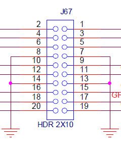
2 1
4 3
etc, but the actually board shows the connections as
1 2
3 4
etc. Which is the correct pinout of J67?
Thanks,
Matty
Solved! Go to Solution.
- Mark as New
- Bookmark
- Subscribe
- Mute
- Subscribe to RSS Feed
- Permalink
- Report Inappropriate Content
The photo you provided corresponds to the Rev.B of the FRWY-LS1046A board which design data (including PCB layout and schematics) is available by the link:
https://www.nxp.com/downloads/en/printed-circuit-boards/FRWY-LS1046A-PA-DF.zip
In the Layerscape FRWY-LS1046A Board Getting Started Guide, Rev. 1 there is photo of the Rev.A (prototype) of the FRWY-LS1046A.
- Mark as New
- Bookmark
- Subscribe
- Mute
- Subscribe to RSS Feed
- Permalink
- Report Inappropriate Content
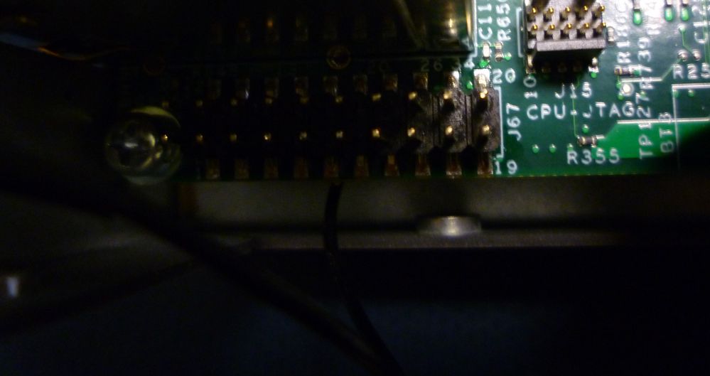
Here is the photo of the actual board. You can clearly see that the pinout is reversed. Look at pins 19 and20 on J67
- Mark as New
- Bookmark
- Subscribe
- Mute
- Subscribe to RSS Feed
- Permalink
- Report Inappropriate Content
The photo you provided corresponds to the Rev.B of the FRWY-LS1046A board which design data (including PCB layout and schematics) is available by the link:
https://www.nxp.com/downloads/en/printed-circuit-boards/FRWY-LS1046A-PA-DF.zip
In the Layerscape FRWY-LS1046A Board Getting Started Guide, Rev. 1 there is photo of the Rev.A (prototype) of the FRWY-LS1046A.
- Mark as New
- Bookmark
- Subscribe
- Mute
- Subscribe to RSS Feed
- Permalink
- Report Inappropriate Content
The request is not clear.
Layerscape FRWY-LS1046A Board Getting Started Guide:
FRWYLS1046A-PA schematics SCH-43607:
Please provide a clear photo and mark the problem position on it.
- Mark as New
- Bookmark
- Subscribe
- Mute
- Subscribe to RSS Feed
- Permalink
- Report Inappropriate Content
Can someone please help? I received an email back from NXP asking for clarification which I sent back in an email. But anyway here is the issue:
The acutal board which I have shows the pinout for the J67 connector as
1 2
3 4
etc.
If I look at the photo on the FRWY getting started guide the photo on there shows
2 1
4 3
etc.
Please verify which is correct?
Thanks!


