
- Forums
- Product Forums
- General Purpose MicrocontrollersGeneral Purpose Microcontrollers
- i.MX Forumsi.MX Forums
- QorIQ Processing PlatformsQorIQ Processing Platforms
- Identification and SecurityIdentification and Security
- Power ManagementPower Management
- Wireless ConnectivityWireless Connectivity
- RFID / NFCRFID / NFC
- Advanced AnalogAdvanced Analog
- Neural Processing UnitsNeural Processing Units
- MCX Microcontrollers
- S32G
- S32K
- S32V
- MPC5xxx
- Other NXP Products
- S12 / MagniV Microcontrollers
- Powertrain and Electrification Analog Drivers
- Sensors
- Vybrid Processors
- Digital Signal Controllers
- 8-bit Microcontrollers
- ColdFire/68K Microcontrollers and Processors
- PowerQUICC Processors
- OSBDM and TBDML
- S32M
- S32Z/E
-
- Solution Forums
- Software Forums
- MCUXpresso Software and ToolsMCUXpresso Software and Tools
- CodeWarriorCodeWarrior
- MQX Software SolutionsMQX Software Solutions
- Model-Based Design Toolbox (MBDT)Model-Based Design Toolbox (MBDT)
- FreeMASTER
- eIQ Machine Learning Software
- Embedded Software and Tools Clinic
- S32 SDK
- S32 Design Studio
- GUI Guider
- Zephyr Project
- Voice Technology
- Application Software Packs
- Secure Provisioning SDK (SPSDK)
- Processor Expert Software
- Generative AI & LLMs
-
- Topics
- Mobile Robotics - Drones and RoversMobile Robotics - Drones and Rovers
- NXP Training ContentNXP Training Content
- University ProgramsUniversity Programs
- Rapid IoT
- NXP Designs
- SafeAssure-Community
- OSS Security & Maintenance
- Using Our Community
-
- Cloud Lab Forums
-
- Knowledge Bases
- ARM Microcontrollers
- i.MX Processors
- Identification and Security
- Model-Based Design Toolbox (MBDT)
- QorIQ Processing Platforms
- S32 Automotive Processing Platform
- Wireless Connectivity
- CodeWarrior
- MCUXpresso Suite of Software and Tools
- MQX Software Solutions
- RFID / NFC
- Advanced Analog
- Neural Processing Units
-
- NXP Tech Blogs
- Home
- :
- MCUXpressoソフトウェアとツール
- :
- LPCXpresso IDE
- :
- Re: Transfer data from parallel GPIO using GPDMA
Transfer data from parallel GPIO using GPDMA
オプション
- RSS フィードを購読する
- トピックを新着としてマーク
- トピックを既読としてマーク
- このトピックを現在のユーザーにフロートします
- ブックマーク
- 購読
- ミュート
- 印刷用ページ
Transfer data from parallel GPIO using GPDMA
06-15-2016
06:42 PM
17,373件の閲覧回数
NXP Employee
- 新着としてマーク
- ブックマーク
- 購読
- ミュート
- RSS フィードを購読する
- ハイライト
- 印刷
- 不適切なコンテンツを報告
Content originally posted in LPCWare by marco on Fri Jul 27 05:55:22 MST 2012
Hi everyone
(sorry for my English!!)
I'm trying to transfer 8bit parallel data input from GPIO pins to SRAM using GPDMA on LPC1850 at 180mhz CCLK. The DMA request is made by counter match.
When I enable the DMA Channel, the Error Interrupt (INTERRSTAT) is asserted, and the DMA channel is disabled.
If I set the SRCADDR register of Channel0 on a FLASH address or a SRAM address the transfer is enabled and properly terminated.
I don't understand what's wrong in the SRCADDR when I initialize it with GPIO PORT.
Below there is my GPDMA initialization.
Can anyone help me for a correct acquisition and DMA initialization?
Thanks in advance.
Hi everyone
(sorry for my English!!)
I'm trying to transfer 8bit parallel data input from GPIO pins to SRAM using GPDMA on LPC1850 at 180mhz CCLK. The DMA request is made by counter match.
When I enable the DMA Channel, the Error Interrupt (INTERRSTAT) is asserted, and the DMA channel is disabled.
If I set the SRCADDR register of Channel0 on a FLASH address or a SRAM address the transfer is enabled and properly terminated.
I don't understand what's wrong in the SRCADDR when I initialize it with GPIO PORT.
Below there is my GPDMA initialization.
// Enable clock and init GPIO inputs LPC_CCU1->CLK_M3_GPIO_CFG = (1<<1) | (1<<0); //enable clock while (!(LPC_CCU1->CLK_M3_GPIO_STAT & (1<<1))); //stat run //for all pins on port 4 I configure input //... LPC_SCU->SFSP9_0 = (0 << 0) | //Function 0 GPIO (2 << 3) | //Disable pullup and pulldown (1 << 5) | //Fast speed (1 << 6) | //Enable input buffer (1 << 7); //Disable input glitch filter //... LPC_CCU1->CLK_M3_DMA_CFG = (1<<1) | (1<<0); //enable clock while (!(LPC_CCU1->CLK_M3_DMA_STAT & (1<<1))); //check stat run // Reset all channel configuration register LPC_GPDMA->C0CONFIG = 0; LPC_GPDMA->C1CONFIG = 0; LPC_GPDMA->C2CONFIG = 0; LPC_GPDMA->C3CONFIG = 0; LPC_GPDMA->C4CONFIG = 0; LPC_GPDMA->C5CONFIG = 0; LPC_GPDMA->C6CONFIG = 0; LPC_GPDMA->C7CONFIG = 0; // Clear all DMA interrupt and error flag LPC_GPDMA->INTTCCLEAR = 0xFF; //Clear CH0 Count Interrupt flag LPC_GPDMA->INTERRCLR = 0xFF; //Clear CH0 Error Interrupt flag // Clear DMA configure LPC_GPDMA->C0CONTROL = 0x00; LPC_GPDMA->C0CONFIG = 0x00; // Assign Linker List Item value LPC_GPDMA->C0LLI = 0; //Assign source address GPIO on port 4 LPC_GPDMA->C0SRCADDR = (uint32_t) &LPC_GPIO_PORT->PIN[4]; //Assign destination address dest1[256] buffer in SRAM LPC_GPDMA->C0DESTADDR = (uint32_t) dest1; LPC_GPDMA->C0CONTROL = (uint32_t)(256 //transfer size | (0 << 12) //source burst size - 1 | (0 << 15) //destination burst size - 1 | (0 << 18) //source width - 8bit | (0 << 21) //dest width - 8bit | (0 << 24) | (0 << 25) | (0 << 26) //source increment - do not inc | (1 << 27) //destination increment - inc | (0 << 28) | (0 << 29) | (0 << 30) | (1 << 31)); //terminal count interrupt - enabled LPC_GPDMA->CONFIG = 1; //Enable GPDMA Controller while (!(LPC_GPDMA->CONFIG & 1)); //check enable LPC_GPDMA->C0CONFIG = 0 //Channel Disable | ((1 & 0x1f) << 1) //source peripheral - Cap0_2 | (0 << 6) //dest request memory - none | (2 << 11) //flow control - peripheral to memory | (1 << 14) //(14) - mask out error interrupt | (1 << 15) //(15) - mask out terminal count interrupt | (0 << 16) //(16) - no locked transfers | (0 << 18); //(18) - no HALT //Enable GPDMA interrupt NVIC_EnableIRQ(DMA_IRQn); LPC_GPDMA->C0CONFIG |= 1; //Channel Enable //Here i received an interrupt error (LPC_GPDMA->INTERRSTAT=1) and the DMA Channel is disabled |
Thanks in advance.
68 返答(返信)
06-15-2016
06:42 PM
5,035件の閲覧回数
NXP Employee
- 新着としてマーク
- ブックマーク
- 購読
- ミュート
- RSS フィードを購読する
- ハイライト
- 印刷
- 不適切なコンテンツを報告
Content originally posted in LPCWare by Parsa on Sun Sep 21 08:52:16 MST 2014
Hi Fred
Thanks,your answer was perfect as always.
I use Timer for capture without interrupts and one IF that check the status of vsync,href, and Timing of pclk.
DMA right now is complicated for me so if you have a example with just interrupts,please send to me.
Thanks
Parsa
Hi Fred
Thanks,your answer was perfect as always.
I use Timer for capture without interrupts and one IF that check the status of vsync,href, and Timing of pclk.
DMA right now is complicated for me so if you have a example with just interrupts,please send to me.
Thanks
Parsa
06-15-2016
06:42 PM
5,035件の閲覧回数
NXP Employee
- 新着としてマーク
- ブックマーク
- 購読
- ミュート
- RSS フィードを購読する
- ハイライト
- 印刷
- 不適切なコンテンツを報告
Content originally posted in LPCWare by Superfred on Sun Sep 21 08:21:17 MST 2014
Hi Parsa,
how did you capture the image, maybe a loop-style program?
The read timing is very critical (if you read too late you capture the next byte), I think this is your problem.
If the processor is handling an interrupt (for example Systick, Uart, ..) loop-style programs are halted and then read too late and the picture is garbled.
The best solution is DMA, here the read timing is independent from the processor. Im my case read at 30FPS at 160x120 resolution is no problem.
The other solution is the use of interrupts, here the PCLK interrupt must be set to high priority, otherwise you will loose bytes again.
I don't think that loop-style programs will ever succed to read camera data!
The next thing: For 160*120(QQVGA) colour resolution you need 38400 Bytes per frame, too much for the 32KB RamAHB32 block starting from 0x2007C000.
I avoid this problem by using only a Black&White images, here I can discard every second Byte in YUYV Format.
I do this by a nice trick: PCLK is connected to CAP1.1, I set LPC_TIM1->MR0 to 2 (instead of 1), so the Timer will drop every second PCLK cycle, so I only read the YY Bytes.
Other solutions: reduce resolution, do not read the whole frame or also use parts of the main RAM.
Conclusion: If you use interrupts or DMA, I can help you with example programs. The requirements to your hardware:
Connect PCLK to a CAP Pin (if possible P1.19=CAP1.1) and VSYNC to any of P0.x or P2.X (if possible P0.8) for Interrupt mode.
Additionally, connect the camera data to P2.0 - P2.7 for DMA.
For loop style programs I don't have examples, and I don't even want to think about any because I doubt they will ever work.
Fred
06-15-2016
06:42 PM
5,034件の閲覧回数
NXP Employee
- 新着としてマーク
- ブックマーク
- 購読
- ミュート
- RSS フィードを購読する
- ハイライト
- 印刷
- 不適切なコンテンツを報告
Content originally posted in LPCWare by Parsa on Sun Sep 21 07:25:03 MST 2014
Hi Fred
thanks for answer. I got a frame without the use of DMA, but the picture is unclear.
I've attached two images.One of them while the lens cap is located.
In your opinion which settings should be changed?
I have QQVGA Resolution and output format is RGB565 and I show pictures in matlab.
also I do not have any color setting.
Parsa
06-15-2016
06:42 PM
5,034件の閲覧回数
NXP Employee
- 新着としてマーク
- ブックマーク
- 購読
- ミュート
- RSS フィードを購読する
- ハイライト
- 印刷
- 不適切なコンテンツを報告
Content originally posted in LPCWare by Superfred on Wed Sep 17 23:56:25 MST 2014
Hi Parsa,
I have never used a loop like yours, because they block everything else.
But I can give you an example with interrupts (a pre-Version of #11), for me much simpler than Loop-Style programs.
All you have to configure the hardware, and it will do nearly all work for you (even more with DMA).
So strongly recommend you to give up this Loop-Style programs and at least use interrupts.
For my example you have to connect PCLK and VSYNC to interruptable ports, but you can leave the Cammera Data Pins as they are now..
If possible connect VSYNC to P0.8 (using GPIO EINT3) and PCLK to P1.19=CAP1.1 (using Timer match interrupt which is also needed for DMA) .
Note: Example #11 also uses interrupts.
Fred
06-15-2016
06:42 PM
5,034件の閲覧回数
NXP Employee
- 新着としてマーク
- ブックマーク
- 購読
- ミュート
- RSS フィードを購読する
- ハイライト
- 印刷
- 不適切なコンテンツを報告
Content originally posted in LPCWare by Parsa on Wed Sep 17 14:10:37 MST 2014
Hello Superfred
I can use that pins. but I have another question.
before using the DMA,can you get the camera data ?
In simple loop like my code?
can you put the example with functions in #11?
thanks
Parsa
Hello Superfred
I can use that pins. but I have another question.
before using the DMA,can you get the camera data ?
In simple loop like my code?
can you put the example with functions in #11?
thanks
Parsa
06-15-2016
06:42 PM
5,034件の閲覧回数
NXP Employee
- 新着としてマーク
- ブックマーク
- 購読
- ミュート
- RSS フィードを購読する
- ハイライト
- 印刷
- 不適切なコンテンツを報告
Content originally posted in LPCWare by Superfred on Wed Sep 17 07:57:12 MST 2014
Hello Parsa,
I use LPC1759, and I also use OV7670 without FIFO, so my code should work for you!
We should start with the hardware:
DMA can't do things like ...>>2, so you have to connect the camera data pins to an GPIO port starting with PX.0, I use P2.0 - P2.7.
DMA needs burst requests, the LPC Timers can generate them. So you need to connect the PCLK Signal to a CAP pin, I use P1.19=CAP1.1.
And it is much easier if you use an Interrupt to monitor VSYNC, I use P0.8 (EINT3).
You can use this or any of Port P0.x or P2.X.
Optional I did 2 things, but they are no must:
-HREF is connected to P1.26=CAP0.0 to count the Lines per Frame in Timer0.
-I noticed that PCLK is still pulsing during the Vertical Blank, so I used an external NC7S08M5 Gate (=74HS08 in SOT-23 Package) to Logical AND PCLK and HREF and feed the resulting signal to CAP1.1, so I don't get blank Camera lines.
Can you also use this Pins (or similar)?
Fred
06-15-2016
06:42 PM
5,034件の閲覧回数
NXP Employee
- 新着としてマーク
- ブックマーク
- 購読
- ミュート
- RSS フィードを購読する
- ハイライト
- 印刷
- 不適切なコンテンツを報告
Content originally posted in LPCWare by Parsa on Tue Sep 16 09:00:57 MST 2014
Hello Superfred
thanks for complete answer.I use lpc1768 and my camera is ov7670 without fifo.
I set up resolution 160*120(QQVGA) and I have 1FPS.
there is problem when I want to capture a frame or even a row of image.
my code is
after that I send each element of qqvgaframe2[] by serial port tp pc
but I only see '0' in PC. With some experimentation, I found that the problem is due to the low rate of transmission from the input port to buffer is defined in RAM.
Because count that defined in loop stay at 5! and program coming out from loop.
Now in your opinion if I use DMA the problem can be solved, or It is better to use RTOS
sorry for my English
and thanks for answer
Hello Superfred
thanks for complete answer.I use lpc1768 and my camera is ov7670 without fifo.
I set up resolution 160*120(QQVGA) and I have 1FPS.
there is problem when I want to capture a frame or even a row of image.
my code is
unsigned char *qqvgaframe2=(unsigned char*)(0x20080000);
camera_QQVGA_RGB565();
while((LPC_GPIO1->FIOPIN&0x10)!=0x10);  //wait until vsync-->low
while((LPC_GPIO1->FIOPIN&0x100)==0x100);   //wait until HREF-->high
while((LPC_GPIO1->FIOPIN&0x100)==0x100){ //stay in loop until HREF-->high
while((LPC_GPIO1->FIOPIN&0x200)==0x200); //wait until pclk-->high
qqvgaframe2=(LPC_GPIO0->FIOPIN>>2); //D0-D7 OV7670 connect to P0.2-P0.9
count=i++;
while((LPC_GPIO1->FIOPIN&0x200)!=0x200);//wait until pclk-->low
} |
after that I send each element of qqvgaframe2[] by serial port tp pc
but I only see '0' in PC. With some experimentation, I found that the problem is due to the low rate of transmission from the input port to buffer is defined in RAM.
Because count that defined in loop stay at 5! and program coming out from loop.
Now in your opinion if I use DMA the problem can be solved, or It is better to use RTOS
sorry for my English
and thanks for answer
06-15-2016
06:42 PM
5,037件の閲覧回数
NXP Employee
- 新着としてマーク
- ブックマーク
- 購読
- ミュート
- RSS フィードを購読する
- ハイライト
- 印刷
- 不適切なコンテンツを報告
Content originally posted in LPCWare by Superfred on Tue Sep 16 05:59:22 MST 2014
Hello Parsa,
my code is already in this thread: post#11, but some registers updated with post#4.
But maybe we should start at the beginning:
Which processor do you have?
What is the resolution of your frame and the frame rate you are planning to have?
To which pins is your Camera connected?
Which Camera Registers do you change with the I2C Bus?
I recommend you to start slow because DMA is not simple:
At first set up low resolution & framerate via I2C (I used 80x60 and 1FPS) and capture via Timer Interrupt (PCLK) to check the connection.
- Note: this will produce only 9600 interrupts per second, well inside the Cortex Mx speed.
Then use the Timer interrupt to fire the DMA and check if you get the DMA terminal count interrupt.
And then transfer real camera data.
If everything works increase resolution & framerate to your need (and memory).
Please feel free to ask me if you have any problems.
Fred
06-15-2016
06:42 PM
5,037件の閲覧回数
NXP Employee
- 新着としてマーク
- ブックマーク
- 購読
- ミュート
- RSS フィードを購読する
- ハイライト
- 印刷
- 不適切なコンテンツを報告
Content originally posted in LPCWare by Parsa on Mon Sep 15 14:00:23 MST 2014
Hi Superfred
I have projects like yours with ov7670. At first for capture a image define some buffer on RAM and without use the DMA ,I read data from input port and transfer to each element of array but this Method was too slow, and I lose data.
I am new in DMA. Can you put the program that get frame by DMA?
thanks
parsa
06-15-2016
06:42 PM
5,037件の閲覧回数
NXP Employee
- 新着としてマーク
- ブックマーク
- 購読
- ミュート
- RSS フィードを購読する
- ハイライト
- 印刷
- 不適切なコンテンツを報告
Content originally posted in LPCWare by HCTEK on Thu Jul 03 03:52:34 MST 2014
Hello superfred,
thanks for your prompt replies.
I will test your sugestions ;)
Best Regards
Hello superfred,
thanks for your prompt replies.
I will test your sugestions ;)
Best Regards
06-15-2016
06:42 PM
5,032件の閲覧回数
NXP Employee
- 新着としてマーク
- ブックマーク
- 購読
- ミュート
- RSS フィードを購読する
- ハイライト
- 印刷
- 不適切なコンテンツを報告
Content originally posted in LPCWare by Superfred on Thu Jul 03 00:13:21 MST 2014
Hello Hugo,
you start a DMA transfer by configuring the registers, but then DMA is doing nothing by itself. After the start you need a DMA Request Signal from a peripheral device to do a burst (a transfer). When the number of DMA Request Signals equals the number in TransferSize the DMA stops.
The LPC clock is much too fast to clock DMA. Use a Timer to generate a clock signal and start at a low rate, you can increase the frequency later.
My idea for your transfer, this works very much like the Camera example but the LPC itself makes the clock:
Use the first Timer to generate the clock signal on a MAT pin. Connect this pin to the FGPA and to the LPC second timer CAP pin. The second Timer will generate the DMA Request Signal like in my camera example.
Transfer setup sequence:
Start the DMA transfer (configure the DMA registers)
Set a GPIO pin High to tell the FGPA that a transfer starts.
Start the first Timer (=the clock).
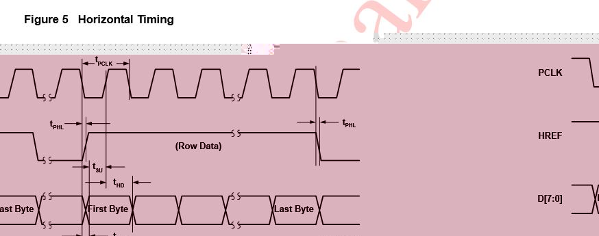
On the positive edge of the clock signal the FGPA writes out the Byte, on the negative edge the DMA reads the data, like the camera timing in the attachment.
The DMA Terminal Count Interrupt turns off the first Timer (=the clock) and the GPIO pin.
The problem here is that the clock can pulse a little longer because the DMA Terminal Count Interrupt needs some time.
This is no problem for the DMA because it already stopped after the number of Clocks configured in TransferSize, but maybe for the FGPA.
You may can do all this with SCT, but there I cannot help you at all.
Fred.
Hello Hugo,
you start a DMA transfer by configuring the registers, but then DMA is doing nothing by itself. After the start you need a DMA Request Signal from a peripheral device to do a burst (a transfer). When the number of DMA Request Signals equals the number in TransferSize the DMA stops.
The LPC clock is much too fast to clock DMA. Use a Timer to generate a clock signal and start at a low rate, you can increase the frequency later.
My idea for your transfer, this works very much like the Camera example but the LPC itself makes the clock:
Use the first Timer to generate the clock signal on a MAT pin. Connect this pin to the FGPA and to the LPC second timer CAP pin. The second Timer will generate the DMA Request Signal like in my camera example.
Transfer setup sequence:
Start the DMA transfer (configure the DMA registers)
Set a GPIO pin High to tell the FGPA that a transfer starts.
Start the first Timer (=the clock).
On the positive edge of the clock signal the FGPA writes out the Byte, on the negative edge the DMA reads the data, like the camera timing in the attachment.
The DMA Terminal Count Interrupt turns off the first Timer (=the clock) and the GPIO pin.
The problem here is that the clock can pulse a little longer because the DMA Terminal Count Interrupt needs some time.
This is no problem for the DMA because it already stopped after the number of Clocks configured in TransferSize, but maybe for the FGPA.
You may can do all this with SCT, but there I cannot help you at all.
Fred.
06-15-2016
06:42 PM
5,032件の閲覧回数
NXP Employee
- 新着としてマーク
- ブックマーク
- 購読
- ミュート
- RSS フィードを購読する
- ハイライト
- 印刷
- 不適切なコンテンツを報告
Content originally posted in LPCWare by HCTEK on Wed Jul 02 08:24:02 MST 2014
Hello superfred ;)
thanks for confirming some of my logic.
The ideia of linked lists to receive data instead of transmit is nice. However it is not the same as declaring a vector with a static size equal to the total size of the linked list and use turn up the Destination Increment Bit?
So in every rising edge of the PCLK signal, the timer turn on a DMA request and a DMA transfer of 8 bits occur. If I am right, in a burst transfer (transfer sizer greater than 1), your timer indicates when each 8 bit transfer need to occur and not only when it must start. The transfer size counter is synchronized with the timer counter request.
Regarding my setup, it is very similar to your camera setup. I am trying to create a parallel interface using DMA to connect my LPC4337 to other chip like a camera or other LPC. The transfer size is also static. The critical point is that I have not a connected pin with a function of a timer in order to test your setup. I was successful connecting my LPC to a FPGA using DMA-M2M. The request was performed using pin interrupts, i.e. a rising edge on a pin will trigger an interrupt and inside of it I start the DMA transfer. Using this setup I think that I only can perform a single DMA transfer since I need to send a signal to the FPGA to update the bus data. I am not sure if this works well if I need to transfer larges amount of data.
In my setup, if I want to perform a burst transfer, each transfer is synchronized with the internal LPC clock? If so maybe I can send that clock to the source and use it to change the bus data.
thanks for the patience superfred,
Best Regards
06-15-2016
06:42 PM
5,032件の閲覧回数
NXP Employee
- 新着としてマーク
- ブックマーク
- 購読
- ミュート
- RSS フィードを購読する
- ハイライト
- 印刷
- 不適切なコンテンツを報告
Content originally posted in LPCWare by Superfred on Wed Jul 02 00:03:13 MST 2014
Hello Hugo,
the OV7670 Camera uses YUYV data format, this means 2 Bytes (=8 Bits) per Pixel, that's why you have 2Bytes * 320 Pixels = 640 Bytes per line.
Because the parallel data bus of the Camera is 8 Bits wide you have to transfer 640 times 8 Bits to capture one line.
So in this case you have to set the TransferSize to 640. After 640 8 Bit transfers the internal DMA counter reaches zero, the transfer stops and (if enabled) the DMA Terminal Count Interrupt is fired.
Note that the maximum TransferSize is 0xFFF, if you need more you need to start in the DMA_IRQHandler a new transfer or use Linked Lists (which I do to capture one whole Frame of 160x105 Pixels which fit's exactly in the 1769's AHB Ram of 32K) .
Now the synchronisation: The Camera sends the PCLK signal to tell the Microcontroller when to read the data: on the positive edge of this signal.
I use this signal to create (with the help of one Timer in Counter mode, no SCT on the LPC1769) the DMA Request Signal, which tells the DMA when to read the data.
Because we have to transfer on each PCLK pulse one time 8 Bits the SBurst Size is 1 and the SWidth is 8.
And to store this Byte into memory also the DBurst Size is 1 and the DWitdh is 8, but we have to turn on the Destination Increment Bit because the next Byte should be written in the next memory location.
Now comes a special thing which I learned just today thanks to your question:
If you set the DBurst Size to 4 and the DWith to 32 (leave SBurst and SWidth at 1 and 8) the DMA controller packs 4 Bytes from the Camera and stores it in one 32 Bit transfer, reducing the amount of DMA to memory transfers by 4! This works only if you have a 32Bit memory Bus and the TransferSize is divideable by 4.
For the synchronisation in your case: Someone have to create a synchronsation signal to tell the other side when the data is (or should be) valid.
In my case it is the Camera with the PCLK signal. If you need help on this you have to tell me more details on your setup.
I hope I understood your question correct and his helps you.
Fred
06-15-2016
06:42 PM
5,032件の閲覧回数
NXP Employee
- 新着としてマーク
- ブックマーク
- 購読
- ミュート
- RSS フィードを購読する
- ハイライト
- 印刷
- 不適切なコンテンツを報告
Content originally posted in LPCWare by HCTEK on Tue Jul 01 08:26:11 MST 2014
Quote: Superfred
Hello Hugo,
as far as i know the only place to manipulate the transfered Bits is LPC_GPDMACHx->DMACCControl SWidth and Dwidth.
If you take 16Bit Width you get in one Burst Bits 0-15, play around with this two settings, maybe it gives you the needed result.
I set both to 8 bit which gives me the correct result: transfer one byte per burst from GPIO P2.0 to P2.7 into memory.
I don't think that DMA gives you the possibility to transfer Bytes/words with other start Bit than 0, you have to use the microcontroller to shift/filter the bits before/after the transfer.
Don't expect too much from DMA, this is just a simple transfer with counters without intelligence.
Fred
Hello,
Thanks for your help superfred. I have another question that maybe you can help me and it is realted with one example that you provide to me (SCTCamDemo)
In that example, a DMA transfer is made in an 8 bit parallel bus. The configuration is as follows:
The transfer size is 2*320, so it is right to say that one DMA transfer will have 2*320*8 bits?
If I am right and relating SBurst(1) <-> SWidth (8) and DBurst(4) <-> DWidth(32), how the source (in this case the camera) will be synchronized with the DMA transfer? It needs to change the bus bits every time the previous 8 bits are in the memory.
The DMA interrupt that indicates the the transfer has finished only goes up after 2*320 transfer?
In general, my question is relating with this. If I want to transfer 10 bytes from GPIO to memory in a 8 bit bus, how can I synchronize the source with the DMA in order to change the bus data 10 times during the transfer.
Best regards,
Quote: Superfred
Hello Hugo,
as far as i know the only place to manipulate the transfered Bits is LPC_GPDMACHx->DMACCControl SWidth and Dwidth.
If you take 16Bit Width you get in one Burst Bits 0-15, play around with this two settings, maybe it gives you the needed result.
I set both to 8 bit which gives me the correct result: transfer one byte per burst from GPIO P2.0 to P2.7 into memory.
I don't think that DMA gives you the possibility to transfer Bytes/words with other start Bit than 0, you have to use the microcontroller to shift/filter the bits before/after the transfer.
Don't expect too much from DMA, this is just a simple transfer with counters without intelligence.
Fred
Hello,
Thanks for your help superfred. I have another question that maybe you can help me and it is realted with one example that you provide to me (SCTCamDemo)
In that example, a DMA transfer is made in an 8 bit parallel bus. The configuration is as follows:
s_ccb.pCHN->CONFIG = // Dis| SrcPerp=SCT | DstRAM | P->M | XferDoneIrqEn 0UL<<0 | YACB_SCTDMAPERIPNUM<<1 | 0UL<<6 | 2UL<<11 | 1UL<<15; s_ccb.pCHN->SRCADDR = (unsigned int )(LPC_GPIO_PORT->PIN + GPT_IMGD0); s_ccb.pCHN->DSTADDR = (unsigned int) s_ccb.pFB; s_ccb.pCHN->CONTROL = //size | SBurst=1| DBurst=4| SWidth=8| DWidth=32| SMstr=1 | DMstr=0 | !SrcInc | DstInc | Prvlg | B,C | EnInt 2*YACB_CAP_W<<0 | 0UL<<12 | 1UL<<15 | 0UL<<18 | 2UL<<21 | 1UL<<24 | 0UL<<25 | 0UL<<26 | 1UL<<27 | 1UL<<28 | 3UL<<29 | 1UL<<31; s_ccb.pCHN->LLI = 0; //(unsigned int) s_ccb.lliAry[0].pNext; // YACB_CAP_W = 320 |
The transfer size is 2*320, so it is right to say that one DMA transfer will have 2*320*8 bits?
If I am right and relating SBurst(1) <-> SWidth (8) and DBurst(4) <-> DWidth(32), how the source (in this case the camera) will be synchronized with the DMA transfer? It needs to change the bus bits every time the previous 8 bits are in the memory.
The DMA interrupt that indicates the the transfer has finished only goes up after 2*320 transfer?
In general, my question is relating with this. If I want to transfer 10 bytes from GPIO to memory in a 8 bit bus, how can I synchronize the source with the DMA in order to change the bus data 10 times during the transfer.
Best regards,
06-15-2016
06:42 PM
5,032件の閲覧回数
NXP Employee
- 新着としてマーク
- ブックマーク
- 購読
- ミュート
- RSS フィードを購読する
- ハイライト
- 印刷
- 不適切なコンテンツを報告
Content originally posted in LPCWare by Superfred on Fri Jun 06 08:37:18 MST 2014
Hello Hugo,
as far as i know the only place to manipulate the transfered Bits is LPC_GPDMACHx->DMACCControl SWidth and Dwidth.
If you take 16Bit Width you get in one Burst Bits 0-15, play around with this two settings, maybe it gives you the needed result.
I set both to 8 bit which gives me the correct result: transfer one byte per burst from GPIO P2.0 to P2.7 into memory.
I don't think that DMA gives you the possibility to transfer Bytes/words with other start Bit than 0, you have to use the microcontroller to shift/filter the bits before/after the transfer.
Don't expect too much from DMA, this is just a simple transfer with counters without intelligence.
Fred
06-15-2016
06:42 PM
5,032件の閲覧回数
NXP Employee
- 新着としてマーク
- ブックマーク
- 購読
- ミュート
- RSS フィードを購読する
- ハイライト
- 印刷
- 不適切なコンテンツを報告
Content originally posted in LPCWare by HCTEK on Fri Jun 06 03:33:39 MST 2014
Quote: Superfred
Hello Hugo,
This example fires 10x per second the Timer3 Match Interrupt, which "clocks" a 10 Byte DMA transfer, which fires 1x per second.
The DMA transfer itself makes nothing reasonable because it is out of sync with the external Camera Clock.
Sorry, the code example is not well commented and formated, so ask me if you don't understand everything.
main() should call DmaSetup() once, then the Interrupt Routines take over and both interrupt counter should increment.
I don't know if LPC_GPDMA->CONFIG & 1 gives you the info if the transfer has finished, I use the DmaTerminalInterrupt to get this information.
If everything is working you can disable the Timer3 Match Interrupt by LPC_TIM3->MCR = 2.
Fred
After some time of deep debug of the registers I was able to perform a request with timer. Sincerely i dont know what I did wrong. I create a new project, I debug again a few times and finally it work!
In fact LPC_GPDMA->CONFIG & 1 does not give me the information that I need. The right expression is LPC_GPDMA->ENBLDCHNS & 1.
Regarding your example, you transfer 8 bits from GPIO port 2 starting from Pin 2.0. The variable PIN has 32 bit, so you read the first 8 rigth? How ca I read the next eigth bits (Pin 2.8 to 2.15) or other bits not starting at Pin 0?
Hugo
06-15-2016
06:42 PM
5,032件の閲覧回数
NXP Employee
- 新着としてマーク
- ブックマーク
- 購読
- ミュート
- RSS フィードを購読する
- ハイライト
- 印刷
- 不適切なコンテンツを報告
Content originally posted in LPCWare by Superfred on Wed Jun 04 22:48:21 MST 2014
Hello Hugo,
I have no experience with LpcOpen, but I can send you a complete "classical" DMA example for the 1769 with internal clock:
This example fires 10x per second the Timer3 Match Interrupt, which "clocks" a 10 Byte DMA transfer, which fires 1x per second.
The DMA transfer itself makes nothing reasonable because it is out of sync with the external Camera Clock.
Sorry, the code example is not well commented and formated, so ask me if you don't understand everything.
main() should call DmaSetup() once, then the Interrupt Routines take over and both interrupt counter should increment.
I don't know if LPC_GPDMA->CONFIG & 1 gives you the info if the transfer has finished, I use the DmaTerminalInterrupt to get this information.
If everything is working you can disable the Timer3 Match Interrupt by LPC_TIM3->MCR = 2.
Fred
Hello Hugo,
I have no experience with LpcOpen, but I can send you a complete "classical" DMA example for the 1769 with internal clock:
#define DMA_Mat3_014
uint32_t Timer3IntCount=0;
uint32_t DMAIntCount=0;
__DATA(RamAHB32) uint8_t CameraBuffer2[16383];

void DmaSetup(void)
{
LPC_SC->PCONP |= (1 << 23);  //Enable Power Timer3
LPC_TIM3->CTCR =0;//Timer Mode
LPC_TIM3->PR = 2500000; //10 Tick/Second (at 25Mhz Peripheral Clock)
LPC_TIM3->MR0 = 1;
LPC_TIM3->MCR = 3;//Interrupt + Reset on match
LPC_TIM3->EMR = 0;//no External match
NVIC_SetPriority( TIMER3_IRQn, 14);
NVIC_EnableIRQ(TIMER3_IRQn);//Enable Interrupt
LPC_TIM3->TCR = 3;//Reset Timer
LPC_TIM3->TCR = 1;//Enable Timer


LPC_SC->PCONP |= (1 << 29);//Enable Power DMA
LPC_SC->DMAREQSEL = 0x40;//DMA Burst Request Input 14 = MAT3.0
LPC_GPDMA->DMACIntTCClear = 0x0F; //Clear DMA channel 0~3 interrupts
LPC_GPDMA->DMACIntErrClr = 0x0F;//Clear DMA channel 0~3 Error interrupts
LPC_GPDMA->DMACConfig = 0x01;/* Enable DMA channels, little endian */
while ( !(LPC_GPDMA->DMACConfig & 0x01) );
NVIC_SetPriority(DMA_IRQn, 30);
NVIC_EnableIRQ(DMA_IRQn);//Enable Interrupt
LPC_TIM3->IR = 1;/* clear Timer interrupt flag */
LPC_GPDMACH0->DMACCSrcAddr = (uint32_t) &LPC_GPIO2->FIOPIN;
LPC_GPDMACH0->DMACCDestAddr = (uintptr_t) CameraBuffer2;
LPC_GPDMACH0->DMACCControl = 10|(0x00 << 12)  //Transfer Size 10
|(0x00 << 15)|(0x00 << 18)|(0x00 << 21)|(1 << 27)|(1 << 31);
LPC_GPDMACH0->DMACCConfig = 0x0C001|(DMA_Mat3_0<<1)|(0x00<<6)|(0x02<<11);
}

void TIMER3_IRQHandler(void)  //Match Register 0 Interrupt
{
LPC_TIM3->IR = 1;/* clear interrupt flag */
Timer3IntCount ++;
}

void DMA_IRQHandler(void)
{
  uint32_t regVal;

  regVal = LPC_GPDMA->DMACIntTCStat;
  if ( regVal )
  {
LPC_GPDMA->DMACIntTCClear = regVal;
if ( regVal & (0x01<<0) )
{
CameraDmaTerminalInterrupt();
}
  regVal = LPC_GPDMA->DMACIntErrStat;
  if ( regVal )
  {
LPC_GPDMA->DMACIntErrClr = regVal;
  }
}

void CameraDmaTerminalInterrupt(void)
{
DMAIntCount++;
LPC_GPDMA->DMACIntTCClear = 0x01<<0;
LPC_GPDMA->DMACIntErrClr = 0x01<<0;
LPC_TIM3->IR = 1;/* clear Timer interrupt flag */
LPC_GPDMACH0->DMACCSrcAddr = (uint32_t) &LPC_GPIO2->FIOPIN;
LPC_GPDMACH0->DMACCDestAddr = (uintptr_t) CameraBuffer2;
LPC_GPDMACH0->DMACCControl = 10|(0x00 << 12)
|(0x00 << 15)|(0x00 << 18)|(0x00 << 21)|(1 << 27)|(1 << 31);
LPC_GPDMACH0->DMACCConfig = 0x0C001|(DMA_Mat3_0<<1)|(0x00<<6)|(0x02<<11);
}
|
This example fires 10x per second the Timer3 Match Interrupt, which "clocks" a 10 Byte DMA transfer, which fires 1x per second.
The DMA transfer itself makes nothing reasonable because it is out of sync with the external Camera Clock.
Sorry, the code example is not well commented and formated, so ask me if you don't understand everything.
main() should call DmaSetup() once, then the Interrupt Routines take over and both interrupt counter should increment.
I don't know if LPC_GPDMA->CONFIG & 1 gives you the info if the transfer has finished, I use the DmaTerminalInterrupt to get this information.
If everything is working you can disable the Timer3 Match Interrupt by LPC_TIM3->MCR = 2.
Fred
06-15-2016
06:42 PM
5,032件の閲覧回数
NXP Employee
- 新着としてマーク
- ブックマーク
- 購読
- ミュート
- RSS フィードを購読する
- ハイライト
- 印刷
- 不適切なコンテンツを報告
Content originally posted in LPCWare by HCTEK on Wed Jun 04 04:23:06 MST 2014
Quote: Superfred
Hello Hugo,
I think the problem is in the Timer config.
In my example I use an external clock connected to CAP3.0 to increment the TC. In your config i see LPC_TIMER3->CTCR = 1, which means your Timer is also in Counter Mode.
Do you supply an external Clock signal?
This all depends on your setup: Who supplies the Clock? In my case it is the OV7670 Camera.
My recomendation: Try to get successfull Timer Match Interrupts before trying GPDMA, so you can distinguish Timer and DMA problems.
Fred
No, i am not using external clock. I change the timer configuration to use LPCOpen funtions and know the timerhandler is activated. The LPC_GPDMA->CONFIG never goes to zero. Also the Handler for DMA and DAC is not activated.
I am using the right procedure to know if the transfer was completed?
Hugo,
Quote: Superfred
Hello Hugo,
I think the problem is in the Timer config.
In my example I use an external clock connected to CAP3.0 to increment the TC. In your config i see LPC_TIMER3->CTCR = 1, which means your Timer is also in Counter Mode.
Do you supply an external Clock signal?
This all depends on your setup: Who supplies the Clock? In my case it is the OV7670 Camera.
My recomendation: Try to get successfull Timer Match Interrupts before trying GPDMA, so you can distinguish Timer and DMA problems.
Fred
No, i am not using external clock. I change the timer configuration to use LPCOpen funtions and know the timerhandler is activated. The LPC_GPDMA->CONFIG never goes to zero. Also the Handler for DMA and DAC is not activated.
I am using the right procedure to know if the transfer was completed?
int main(void)
{
uint32_t timerFreq;
uint32_t i;
uint32_t triangle[32];

SystemCoreClockUpdate();
Board_Init();

Chip_SCU_DAC_Analog_Config(); // Enable DAC function on P4.4
Chip_DAC_Init(LPC_DAC); //DAC Init
Chip_DAC_SetDMATimeOut(LPC_DAC, 0x1); //set time out for DAC
Chip_DAC_ConfigDAConverterControl(LPC_DAC, (DAC_CNT_ENA | DAC_DMA_ENA));

/* Enable timer3 clock and reset it */
Chip_TIMER_Init(LPC_TIMER3);
Chip_RGU_TriggerReset(RGU_TIMER3_RST);
while (Chip_RGU_InReset(RGU_TIMER3_RST)) {}

/* Get timer 3 peripheral clock rate = 204Mhz */
timerFreq = Chip_Clock_GetRate(CLK_MX_TIMER3);
/* Timer setup for match and interrupt at TICKRATE_HZ = 1000 */
/*Chip_TIMER_Reset(LPC_TIMER3);
LPC_TIMER3->MR[1] = timerFreq / TICKRATE_HZ;
LPC_TIMER3->MCR = 0x0003;
LPC_TIMER3->CTCR = 0;
LPC_TIMER3->EMR = 0x0031;
LPC_TIMER3->TCR = 2;*/
Chip_TIMER_Reset(LPC_TIMER3);
Chip_TIMER_MatchEnableInt(LPC_TIMER3, 1);
Chip_TIMER_SetMatch(LPC_TIMER3, 1, (timerFreq / TICKRATE_HZ));
Chip_TIMER_ResetOnMatchEnable(LPC_TIMER3, 1);
//Chip_TIMER_Enable(LPC_TIMER3);

/*triangular wave*/
for(i=0; i!=16; i++) triangle = (uint32_t) (DAC_VALUE((((i+1)) - 1)) | DAC_BIAS_EN);
for(i=0; i!=16; i++) triangle[16+i] = (uint32_t) (DAC_VALUE((((16-i)) - 64)) | DAC_BIAS_EN);
for (i = 0; i < 0x10000; i++){}

while(1){
/* Initialize GPDMA controller */
Chip_GPDMA_Init(LPC_GPDMA);
LPC_GPDMA->CONFIG =  1;          // enable
while (!(LPC_GPDMA->CONFIG & 1)) {}

LPC_CREG->DMAMUX = 0 << (2 * 8); //Timer 3 match 1
    LPC_GPDMA->CH[0].SRCADDR  = (uint32_t) (&triangle);
    LPC_GPDMA->CH[0].DESTADDR = (uint32_t) (&LPC_DAC->CR);
    LPC_GPDMA->CH[0].LLI = 0;
    LPC_GPDMA->CH[0].CONTROL  = 32           // transfer size (0 - 11) = 32
                            | (0 << 12)        // source burst size (12 - 14) = 1
                            | (0 << 15)        // destination burst size (15 - 17) = 1
                            | (2 << 18)        // source width (18 - 20) = 32 bit
                            | (2 << 21)        // destination width (21 - 23) = 32 bit
                            | (0 << 24)        // source AHB select (24) = AHB 0
                            | (1 << 25)        // destination AHB select (25) = AHB 1
                            | (1 << 26)        // source increment (26) = increment
                            | (0 << 27)        // destination increment (27) = no increment
                            | (0 << 28)        // mode select (28) = access in user mode
                            | (0 << 29)        // (29) = access not bufferable
                            | (0 << 30)        // (30) = access not cacheable
                            | (0 << 31);       // terminal count interrupt disabled

    LPC_GPDMA->CH[0].CONFIG   =  1           // channel enabled (0)
                            | (0 << 1)         // source peripheral (1 - 5) = memory
                            | (8 << 6)         // destination request peripheral (6 - 10) = //Timer 3 match 1
                            | (1 << 11)        // flow control (11 - 13) = mem to per
                            | (0 << 14)        // (14) = mask out error interrupt
                            | (0 << 15)        // (15) = mask out terminal count interrupt
                            | (0 << 16)        // (16) = no locked transfers
                            | (0 << 18);       // (27) = no HALT

Chip_TIMER_Enable(LPC_TIMER3);

/* Enable timer, DMA, DAC interrupt */
NVIC_ClearPendingIRQ(TIMER3_IRQn);
NVIC_EnableIRQ(TIMER3_IRQn);
NVIC_ClearPendingIRQ(DMA_IRQn);
NVIC_EnableIRQ(DMA_IRQn);
NVIC_ClearPendingIRQ(DAC_IRQn);
NVIC_EnableIRQ(DAC_IRQn);

while( LPC_GPDMA->CONFIG & 1){ // wait until transfer is completed
Board_LED_Toggle(2);
}
Chip_TIMER_Disable(LPC_TIMER3);
}

return 0;
} |
Hugo,
06-15-2016
06:42 PM
5,032件の閲覧回数
NXP Employee
- 新着としてマーク
- ブックマーク
- 購読
- ミュート
- RSS フィードを購読する
- ハイライト
- 印刷
- 不適切なコンテンツを報告
Content originally posted in LPCWare by Superfred on Tue Jun 03 07:48:21 MST 2014
Hello Hugo,
I think the problem is in the Timer config.
In my example I use an external clock connected to CAP3.0 to increment the TC. In your config i see LPC_TIMER3->CTCR = 1, which means your Timer is also in Counter Mode.
Do you supply an external Clock signal?
This all depends on your setup: Who supplies the Clock? In my case it is the OV7670 Camera.
My recomendation: Try to get successfull Timer Match Interrupts before trying GPDMA, so you can distinguish Timer and DMA problems.
Fred
06-15-2016
06:42 PM
5,032件の閲覧回数
NXP Employee
- 新着としてマーク
- ブックマーク
- 購読
- ミュート
- RSS フィードを購読する
- ハイライト
- 印刷
- 不適切なコンテンツを報告
Content originally posted in LPCWare by HCTEK on Tue Jun 03 07:22:34 MST 2014
Hello,
before I went to test a parallel transfer, i tried some examples that I found in LPCOpen. From what i saw, the examples on LPCOpen uses the destination peripheral as request peripheral. Since I want to use an external signal to perform the request, I need to use change the request peripheral.
Similar as Superfred code above, I tried use timers to perform that request, however, without success. In my example, the ouput is the DAC. The micro is LPC4337.
The problem that I found is that the condition " LPC_GPDMA->CONFIG & 1" never goes zero, which means that the transfer did not finish
What I am doing wrong?
Thanks in advance,
Hugo
Hello,
before I went to test a parallel transfer, i tried some examples that I found in LPCOpen. From what i saw, the examples on LPCOpen uses the destination peripheral as request peripheral. Since I want to use an external signal to perform the request, I need to use change the request peripheral.
Similar as Superfred code above, I tried use timers to perform that request, however, without success. In my example, the ouput is the DAC. The micro is LPC4337.
The problem that I found is that the condition " LPC_GPDMA->CONFIG & 1" never goes zero, which means that the transfer did not finish
What I am doing wrong?
int main(void)
{
uint32_t timerFreq;
uint32_t i;
uint32_t triangle[32];

SystemCoreClockUpdate();
Board_Init();

Chip_SCU_DAC_Analog_Config(); // Enable DAC function on P4.4
Chip_DAC_Init(LPC_DAC); //DAC Init
Chip_DAC_SetDMATimeOut(LPC_DAC, 0x1); //set time out for DAC
Chip_DAC_ConfigDAConverterControl(LPC_DAC, (DAC_CNT_ENA | DAC_DMA_ENA));

/* Enable timer3 clock and reset it */
Chip_TIMER_Init(LPC_TIMER3);
Chip_RGU_TriggerReset(RGU_TIMER3_RST);
while (Chip_RGU_InReset(RGU_TIMER3_RST)) {}

/* Get timer 3 peripheral clock rate = 204Mhz */
timerFreq = Chip_Clock_GetRate(CLK_MX_TIMER3);
/* Timer setup for match and interrupt at TICKRATE_HZ = 1000 */
Chip_TIMER_Reset(LPC_TIMER3);
LPC_TIMER3->MR[1] = timerFreq / TICKRATE_HZ;
LPC_TIMER3->MCR = 0x0003;
LPC_TIMER3->CTCR = 1;
LPC_TIMER3->EMR = 0x0031;
LPC_TIMER3->TCR = 2;

/*triangular wave*/
for(i=0; i!=16; i++) triangle = (uint32_t) (DAC_VALUE((((i+1)) - 1)) | DAC_BIAS_EN);
for(i=0; i!=16; i++) triangle[16+i] = (uint32_t) (DAC_VALUE((((16-i)) - 64)) | DAC_BIAS_EN);
for (i = 0; i < 0x10000; i++){}

while(1){
/* Initialize GPDMA controller */
Chip_GPDMA_Init(LPC_GPDMA);
LPC_GPDMA->CONFIG =  1;          // enable
while (!(LPC_GPDMA->CONFIG & 1)) {}

LPC_CREG->DMAMUX = 0 << (2 * 8); //Timer 3 match 1
    LPC_GPDMA->CH[0].SRCADDR  = (uint32_t) (&triangle);
    LPC_GPDMA->CH[0].DESTADDR = (uint32_t) (&LPC_DAC->CR);
    LPC_GPDMA->CH[0].LLI = 0;
    LPC_GPDMA->CH[0].CONTROL  = 32           // transfer size (0 - 11) = 32
                            | (0 << 12)        // source burst size (12 - 14) = 1
                            | (0 << 15)        // destination burst size (15 - 17) = 1
                            | (2 << 18)        // source width (18 - 20) = 32 bit
                            | (2 << 21)        // destination width (21 - 23) = 32 bit
                            | (0 << 24)        // source AHB select (24) = AHB 0
                            | (1 << 25)        // destination AHB select (25) = AHB 1
                            | (1 << 26)        // source increment (26) = increment
                            | (0 << 27)        // destination increment (27) = no increment
                            | (0 << 28)        // mode select (28) = access in user mode
                            | (0 << 29)        // (29) = access not bufferable
                            | (0 << 30)        // (30) = access not cacheable
                            | (0 << 31);       // terminal count interrupt disabled

    LPC_GPDMA->CH[0].CONFIG   =  1           // channel enabled (0)
                            | (0 << 1)         // source peripheral (1 - 5) = memory
                            | (8 << 6)         // destination request peripheral (6 - 10) = //Timer 3 match 1
                            | (1 << 11)        // flow control (11 - 13) = mem to per
                            | (0 << 14)        // (14) = mask out error interrupt
                            | (0 << 15)        // (15) = mask out terminal count interrupt
                            | (0 << 16)        // (16) = no locked transfers
                            | (0 << 18);       // (27) = no HALT

/* Start the DMA channel */
Chip_GPDMA_ChannelCmd(LPC_GPDMA, 0, ENABLE);

Chip_TIMER_Enable(LPC_TIMER3);

/* Enable timer and DMA interrupt */
NVIC_ClearPendingIRQ(TIMER3_IRQn);
NVIC_EnableIRQ(TIMER3_IRQn);
NVIC_ClearPendingIRQ(DMA_IRQn);
NVIC_EnableIRQ(DMA_IRQn);


while( LPC_GPDMA->CONFIG & 1){ // wait until transfer is completed
Board_LED_Toggle(2);
}
Chip_TIMER_Disable(LPC_TIMER3);
}

return 0;
} |
Thanks in advance,
Hugo
06-15-2016
06:42 PM
5,032件の閲覧回数
NXP Employee
- 新着としてマーク
- ブックマーク
- 購読
- ミュート
- RSS フィードを購読する
- ハイライト
- 印刷
- 不適切なコンテンツを報告
Content originally posted in LPCWare by HCTEK on Wed May 28 07:36:07 MST 2014
Thanks for the reply superfred, these examples will for sure help me.
I will look them and test some procedures. For sure I will need more help further ;).
Best Regards
Thanks for the reply superfred, these examples will for sure help me.
I will look them and test some procedures. For sure I will need more help further ;).
Best Regards