
- Forums
- Product Forums
- General Purpose MicrocontrollersGeneral Purpose Microcontrollers
- i.MX Forumsi.MX Forums
- QorIQ Processing PlatformsQorIQ Processing Platforms
- Identification and SecurityIdentification and Security
- Power ManagementPower Management
- Wireless ConnectivityWireless Connectivity
- RFID / NFCRFID / NFC
- Advanced AnalogAdvanced Analog
- Neural Processing UnitsNeural Processing Units
- MCX Microcontrollers
- S32G
- S32K
- S32V
- MPC5xxx
- Other NXP Products
- S12 / MagniV Microcontrollers
- Powertrain and Electrification Analog Drivers
- Sensors
- Vybrid Processors
- Digital Signal Controllers
- 8-bit Microcontrollers
- ColdFire/68K Microcontrollers and Processors
- PowerQUICC Processors
- OSBDM and TBDML
- S32M
- S32Z/E
-
- Solution Forums
- Software Forums
- MCUXpresso Software and ToolsMCUXpresso Software and Tools
- CodeWarriorCodeWarrior
- MQX Software SolutionsMQX Software Solutions
- Model-Based Design Toolbox (MBDT)Model-Based Design Toolbox (MBDT)
- FreeMASTER
- eIQ Machine Learning Software
- Embedded Software and Tools Clinic
- S32 SDK
- S32 Design Studio
- GUI Guider
- Zephyr Project
- Voice Technology
- Application Software Packs
- Secure Provisioning SDK (SPSDK)
- Processor Expert Software
- Generative AI & LLMs
-
- Topics
- Mobile Robotics - Drones and RoversMobile Robotics - Drones and Rovers
- NXP Training ContentNXP Training Content
- University ProgramsUniversity Programs
- Rapid IoT
- NXP Designs
- SafeAssure-Community
- OSS Security & Maintenance
- Using Our Community
-
- Cloud Lab Forums
-
- Knowledge Bases
- ARM Microcontrollers
- i.MX Processors
- Identification and Security
- Model-Based Design Toolbox (MBDT)
- QorIQ Processing Platforms
- S32 Automotive Processing Platform
- Wireless Connectivity
- CodeWarrior
- MCUXpresso Suite of Software and Tools
- MQX Software Solutions
- RFID / NFC
- Advanced Analog
- Neural Processing Units
-
- NXP Tech Blogs
- Home
- :
- General Purpose Microcontrollers
- :
- LPC Microcontrollers
- :
- Unable to connect to LPC8N04 dev board
Unable to connect to LPC8N04 dev board
- Subscribe to RSS Feed
- Mark Topic as New
- Mark Topic as Read
- Float this Topic for Current User
- Bookmark
- Subscribe
- Mute
- Printer Friendly Page
Unable to connect to LPC8N04 dev board
- Mark as New
- Bookmark
- Subscribe
- Mute
- Subscribe to RSS Feed
- Permalink
- Report Inappropriate Content

I was using the dev board just fine and was able to flash firmware without issue from mcuexpresso. Now, I get the above error when trying to flash new firmware or even just trying to perform a mass erase. The firmware I flashed just before becoming unable to interact with the board was one of the i2c examples that I had modified by a couple of lines in main. Pressing the reset button on the board doesn't help.
The P7 and P8 headers are in the correct position for SWD.
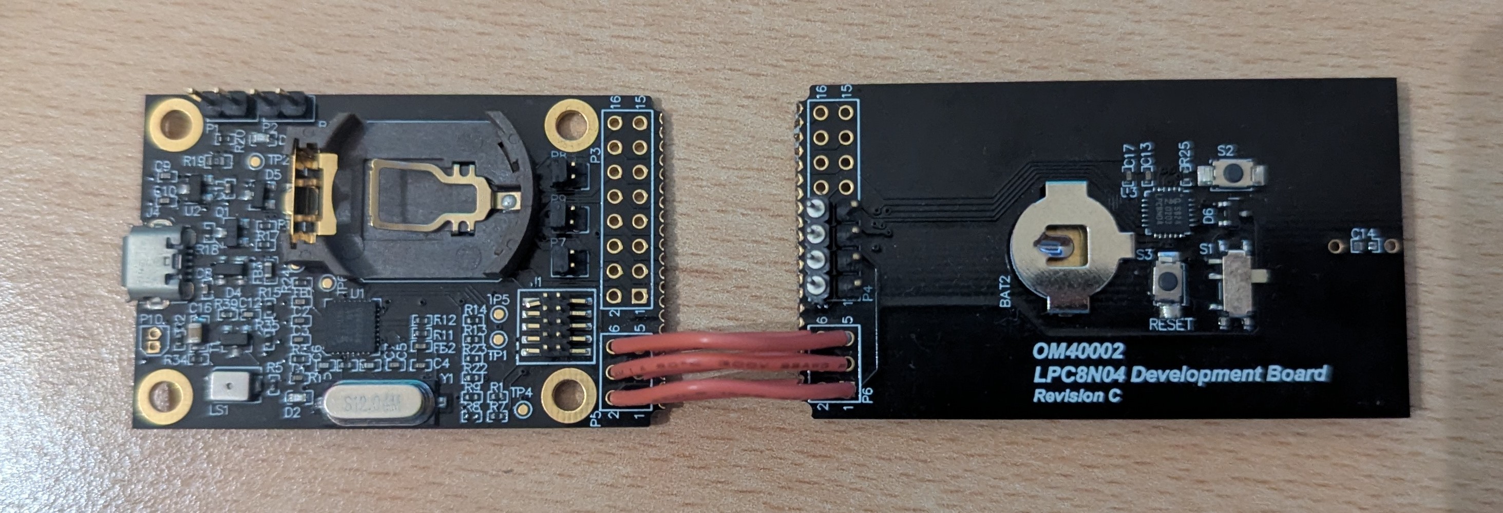
I have split the board in two and soldered wires across P6 and P5 but I have just checked all the connections with a multimeter and I don't find any shorts or disconnections.
- Mark as New
- Bookmark
- Subscribe
- Mute
- Subscribe to RSS Feed
- Permalink
- Report Inappropriate Content
Hello @TheOrangeTeaFrog
If CRP is not the issue, please try updating the debugger firmware on the board as follows:
Connect P2 with a jumper, then repower the board. Click the "Boot Debug Probe" button on MCUXpresso IDE.

After a successful update, import a simple GPIO demo under SDK and try debugging again.
BR
Alice
- Mark as New
- Bookmark
- Subscribe
- Mute
- Subscribe to RSS Feed
- Permalink
- Report Inappropriate Content
Hello @Alice_Yang , thanks again for the help.
I have downloaded new firmware from the NXP website. From the "LPC8N04 Development Board for LPC8N04 MCU" product page I downloaded "LPC11Uxx-Debug-Probe-VCOM". This contained "firmware.bin".
I tried the method you suggest, but after clicking the "Boot debug probe" option, it was not clear what I needed to do next.
I referred to "UM11082-Dev-Board-User-Manual.pdf" which contains a section on updating the firmware. It suggests bridging the P2 header, powering the board, deleting the firmware from the USB device "CRP_DISABLED", copying the newly downloaded firmware to the device, removing the jumper and repowering the board.
I successfully completed all these steps. However, now the board isn't even recognised by my computer as a USB device. If I reconnect the P2 header, it shows up as a usb storage device so I am able to try flashing the debugger firmware again. However, as soon as I remove the P2 header, my computer now no longer recognised it at all.
Is it possible that I have downloaded the wrong firmware?
- Mark as New
- Bookmark
- Subscribe
- Mute
- Subscribe to RSS Feed
- Permalink
- Report Inappropriate Content

BR
Alice
- Mark as New
- Bookmark
- Subscribe
- Mute
- Subscribe to RSS Feed
- Permalink
- Report Inappropriate Content
Hi @Alice_Yang
I think I might have removed the P2 header before powering off, or not unmounted correctly. Anyways, today I have been able to flash the new debugger firmware to the device and, after removing P2 and power cycling, it is recognised by the PC. I am now back to the situation at the start of my post: "Cannot provide power to DAP bus" when trying to flash or mass erase.
I am using Linux but also tried this on a Windows machine to see how it shows in the device manager and noticed some interesting things. First, the device (after being flashed with new debugger firmware) does not appear in the device manager in the same way as your screenshot. Rather than showing "NXP LPC11Uxx VCOM" it just shows "USB Serial Device". I installed the windows driver for the board which was downloaded as part of the same .zip file as firmware.bin. I also installed mcuexpresso on the machine and installed the relevant SDK. After this, I restarted the Windows machine and the device still shows as "USB Serial Device". I know this is the correct device since it disappears/reappears as I unplug and replug the device.
Next, I tried to flash some example code as well as performing a mass erase from mcuexpresso on Windows. This produces the same result as on Linux: "Cannot provide power to DAP bus" but gives a little more context. After clicking on the gui flash button, it searches for debug probes and finds my device. Then it brings up a dialog that allows me to select between performing an erase or flashing some firmware I have built. After this, I get a new dialog called "SWD Configuration" which shows "0 available SWD Devices detected. Connect a device and try again". I then get the usual "Cannot provide power to DAP bus" error.
I am not sure why the "SWD Configuration" dialog only appear on Windows. I have checked the SWD header pins again and they are definitely all correctly placed to enable SWD. I have also performed another continuity test with a multimeter and found no issues. It seems that there is still something wrong.
I was also able to attach a logic probe to the SWCLK, SWDIO and NFC_RESET pins as I attempt to perform a mass erase from MCUexpresso

From top to bottom: SWDIO, SWCLK, RFC_RESET
I don't know enough about SWD to determine if there is an issue here
- Mark as New
- Bookmark
- Subscribe
- Mute
- Subscribe to RSS Feed
- Permalink
- Report Inappropriate Content
Hello @TheOrangeTeaFrog
-
Take a video showing all your steps. Include the Device Manager when you connect the board.
-
Take a photo of your board.
Thank you.
BR
Alice
- Mark as New
- Bookmark
- Subscribe
- Mute
- Subscribe to RSS Feed
- Permalink
- Report Inappropriate Content
Hi @Alice_Yang Please find a video and image attached.
Something I noticed was that the error I get when I try the first time is a bit different to subsequent times. In the video, I attempt 3 times: I get a different error on the first attempt compared to attempt 2 and 3. If I keep going, I get the same error from attempt 2/3 over and over forever. Until I restart
- Mark as New
- Bookmark
- Subscribe
- Mute
- Subscribe to RSS Feed
- Permalink
- Report Inappropriate Content
I cannot see the connection very clearly. Please connect the pins on P5 with those on P6, and do not connect them to the small pad on the left.


Thank you.
BR
Alice
- Mark as New
- Bookmark
- Subscribe
- Mute
- Subscribe to RSS Feed
- Permalink
- Report Inappropriate Content
Hi Alice
Apologies if the first photo wasn't clear. The wires are soldered into the holes in the board.
As far as I can tell, my wiring is the same as your diagram.
Additionally, the board was functioning correctly for quite some time with this exact wiring.
I have check for continutity/shorts by placing multimeter probes across the 10 pin debug connector to the solder points on p6 and all seems fine.

- Mark as New
- Bookmark
- Subscribe
- Mute
- Subscribe to RSS Feed
- Permalink
- Report Inappropriate Content
Based on all our discussions, if debugging could be done normally before and CRP was never enabled, it means that the chip LPC8n04 on your board is broken.
BR
Alice
- Mark as New
- Bookmark
- Subscribe
- Mute
- Subscribe to RSS Feed
- Permalink
- Report Inappropriate Content
Do you have any why it might broken? Would it have been something I did or are there QC issues with this chip? I am evaluating this chip for inclusion in our next product so this is concerning for me. Do you offer other NFC child that would be less likely to break?
- Mark as New
- Bookmark
- Subscribe
- Mute
- Subscribe to RSS Feed
- Permalink
- Report Inappropriate Content
https://community.nxp.com/t5/forums/postpage/choose-node/true/board-id/nfc

BR
Alice
- Mark as New
- Bookmark
- Subscribe
- Mute
- Subscribe to RSS Feed
- Permalink
- Report Inappropriate Content
Hi Alice, are you saying that setting CRP2 or CRP3 permanently disables SWD and makes it impossible to flash any more firmware to the device effectively destroying it? I didn't find any warnings about this in the documentation so I find this surprising.
- Mark as New
- Bookmark
- Subscribe
- Mute
- Subscribe to RSS Feed
- Permalink
- Report Inappropriate Content

By the way, has your board ever been debug well after splitting it?
BR
Alice
- Mark as New
- Bookmark
- Subscribe
- Mute
- Subscribe to RSS Feed
- Permalink
- Report Inappropriate Content
Hi Alice, you are right, I have tried that. I got confused between the SWD stuff and the idea of the board being broken.
After splitting the board, I have had no issues. I have been able to program and debug fine for weeks.
- Mark as New
- Bookmark
- Subscribe
- Mute
- Subscribe to RSS Feed
- Permalink
- Report Inappropriate Content
You can also check whether the wires soldered into the holes on the board have become disconnected after several weeks. If no such issue is found, I suspect the chip may be broken.
BR
Alice
- Mark as New
- Bookmark
- Subscribe
- Mute
- Subscribe to RSS Feed
- Permalink
- Report Inappropriate Content
Hi @Alice_Yang
I order a new at your recommendation board and I am having the exact same issue again.
Here is exactly what has happened with the new board:
- I took the board out of the packaging.
- I soldered 4 header pins to P4 pins 1 (SCL), 3 (SDA), 5 (VCC), 7 (GND)
- I connected the board via usb to my PC
- I saw that the example code that is preloaded on the board was running: the LED array on the back was lighting up.
- I moved the jumpers on P7 and P8 to the SWD position
- I loaded up the i2c_polling_transfer_master example and flashed this onto the board
- I saw the LED go dark which suggested this worked. I got no errors in MCUExpresso when doing this.
- I connected my logic debug probe and pull up resistors to the I2C pins in the hopes of seeing the I2C signal. I put a 30k resistor between SDA and VCC and another 30k resistor between SCL and VCC. I connected my debug probe to SDA and SCL.
- I pressed the reset button the chip while recording logic. I saw no changes to the SDA/SCL logic lines.
- I tried to flash the board again. I now get errors like before

Nothing I do seems to fix these errors. I have tried different USB cables, unplugging and replugging the board, removing and reinserting the SWD headers, resetting the board via the reset button, restarting MCUexpresso.
The thing that seems most likely to have triggered this would be connecting the pull up resistors but I do not see how this would have fried the chip.
- Mark as New
- Bookmark
- Subscribe
- Mute
- Subscribe to RSS Feed
- Permalink
- Report Inappropriate Content
Please check what CRP value do you setting. If it is CRP2 or CRP3 as below, SWD access is disabled.

Please check the CRP value you are setting. If it is CRP2 or CRP3 as shown below, SWD access will be disabled.
BR
Alice
- Mark as New
- Bookmark
- Subscribe
- Mute
- Subscribe to RSS Feed
- Permalink
- Report Inappropriate Content
Hello @Alice_Yang , thanks for the reply
I can see that the file startup_lpc8n04.c (part of the lpc8n04devboard_lpc_i2c_1_polling_transfer_master example) sets the value of the CRP to NO_CRP.
However, I can also seen in the .map file that results from building the project that the .crp section is listed under the "Discarded input sections". Running readelf on the resulting binary also shows no CRP symbol or .crp section.
While I could manually edit the linker script to ensure the section is included, it seems that the linker script is automatically generated by mcuexpresso. Is there somewhere in the IDE where I need to configure something to do with the CRP?
Thanks