- Forums
- Product Forums
- General Purpose MicrocontrollersGeneral Purpose Microcontrollers
- i.MX Forumsi.MX Forums
- QorIQ Processing PlatformsQorIQ Processing Platforms
- Identification and SecurityIdentification and Security
- Power ManagementPower Management
- Wireless ConnectivityWireless Connectivity
- RFID / NFCRFID / NFC
- Advanced AnalogAdvanced Analog
- MCX Microcontrollers
- S32G
- S32K
- S32V
- MPC5xxx
- Other NXP Products
- S12 / MagniV Microcontrollers
- Powertrain and Electrification Analog Drivers
- Sensors
- Vybrid Processors
- Digital Signal Controllers
- 8-bit Microcontrollers
- ColdFire/68K Microcontrollers and Processors
- PowerQUICC Processors
- OSBDM and TBDML
- S32M
- S32Z/E
-
- Solution Forums
- Software Forums
- MCUXpresso Software and ToolsMCUXpresso Software and Tools
- CodeWarriorCodeWarrior
- MQX Software SolutionsMQX Software Solutions
- Model-Based Design Toolbox (MBDT)Model-Based Design Toolbox (MBDT)
- FreeMASTER
- eIQ Machine Learning Software
- Embedded Software and Tools Clinic
- S32 SDK
- S32 Design Studio
- GUI Guider
- Zephyr Project
- Voice Technology
- Application Software Packs
- Secure Provisioning SDK (SPSDK)
- Processor Expert Software
- Generative AI & LLMs
-
- Topics
- Mobile Robotics - Drones and RoversMobile Robotics - Drones and Rovers
- NXP Training ContentNXP Training Content
- University ProgramsUniversity Programs
- Rapid IoT
- NXP Designs
- SafeAssure-Community
- OSS Security & Maintenance
- Using Our Community
-
- Cloud Lab Forums
-
- Knowledge Bases
- ARM Microcontrollers
- i.MX Processors
- Identification and Security
- Model-Based Design Toolbox (MBDT)
- QorIQ Processing Platforms
- S32 Automotive Processing Platform
- Wireless Connectivity
- CodeWarrior
- MCUXpresso Suite of Software and Tools
- MQX Software Solutions
- RFID / NFC
- Advanced Analog
-
- NXP Tech Blogs
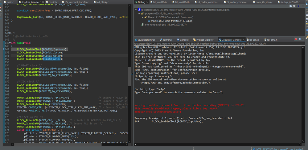
Suspended on enable clock for InputMux.
Hello.
I use LPC55s36 with unmodified i2s_dma_transfer example. From default pins i shorted JP3 1-2, JP53 1-2 and JP50 1-2, like the example says to do. Terminal says that it went throught all of the code and, theres no errors in terminal. Terminal:
Configure codec
Configure I2S
Setup looping playback of sine wave
But i can't hear anything in headphones. What could be the issue?
Hi @CzyzyK
You can observe the output effect through an oscilloscope.
According to the schematic, you can measure these three signals.
The above is the result of my test, you can refer to it.
BR
Hang
Hi @CzyzyK
I checked the lpc55s36_i2s_dma_transfer demo readme.
Board settings
==============
Short JP50 1-2,JP53 1-2
But in your setting,
"From default pins i shorted JP3 1-2, JP53 1-2 and JP50 1-2, like the example says to do. "
Why shorted JP3 1-2?
BR
Hang
Hi @CzyzyK
1. For CDC_I2S1_RX_BCLK_OnBoard signal, you can measure the J9 Pin16.
2. For CDC_FC7_I2S_TX_OnBoard signal, you can measure the J22 Pin2.
3. For CDC_I2S_WS_OnBoard signal, you can measure the J22 Pin4.
BR
Hang


