- Forums
- Product Forums
- General Purpose MicrocontrollersGeneral Purpose Microcontrollers
- i.MX Forumsi.MX Forums
- QorIQ Processing PlatformsQorIQ Processing Platforms
- Identification and SecurityIdentification and Security
- Power ManagementPower Management
- Wireless ConnectivityWireless Connectivity
- RFID / NFCRFID / NFC
- Advanced AnalogAdvanced Analog
- MCX Microcontrollers
- S32G
- S32K
- S32V
- MPC5xxx
- Other NXP Products
- S12 / MagniV Microcontrollers
- Powertrain and Electrification Analog Drivers
- Sensors
- Vybrid Processors
- Digital Signal Controllers
- 8-bit Microcontrollers
- ColdFire/68K Microcontrollers and Processors
- PowerQUICC Processors
- OSBDM and TBDML
- S32M
- S32Z/E
-
- Solution Forums
- Software Forums
- MCUXpresso Software and ToolsMCUXpresso Software and Tools
- CodeWarriorCodeWarrior
- MQX Software SolutionsMQX Software Solutions
- Model-Based Design Toolbox (MBDT)Model-Based Design Toolbox (MBDT)
- FreeMASTER
- eIQ Machine Learning Software
- Embedded Software and Tools Clinic
- S32 SDK
- S32 Design Studio
- GUI Guider
- Zephyr Project
- Voice Technology
- Application Software Packs
- Secure Provisioning SDK (SPSDK)
- Processor Expert Software
- Generative AI & LLMs
-
- Topics
- Mobile Robotics - Drones and RoversMobile Robotics - Drones and Rovers
- NXP Training ContentNXP Training Content
- University ProgramsUniversity Programs
- Rapid IoT
- NXP Designs
- SafeAssure-Community
- OSS Security & Maintenance
- Using Our Community
-
- Cloud Lab Forums
-
- Knowledge Bases
- ARM Microcontrollers
- i.MX Processors
- Identification and Security
- Model-Based Design Toolbox (MBDT)
- QorIQ Processing Platforms
- S32 Automotive Processing Platform
- Wireless Connectivity
- CodeWarrior
- MCUXpresso Suite of Software and Tools
- MQX Software Solutions
- RFID / NFC
- Advanced Analog
-
- NXP Tech Blogs
- Home
- :
- General Purpose Microcontrollers
- :
- LPC Microcontrollers
- :
- Re: RTC calibration in LPC54608J512BD208
RTC calibration in LPC54608J512BD208
- Subscribe to RSS Feed
- Mark Topic as New
- Mark Topic as Read
- Float this Topic for Current User
- Bookmark
- Subscribe
- Mute
- Printer Friendly Page
RTC calibration in LPC54608J512BD208
- Mark as New
- Bookmark
- Subscribe
- Mute
- Subscribe to RSS Feed
- Permalink
- Report Inappropriate Content
Hi,
Can someone share the process of calibrating RTC of LPC54608J512BD208.
I am using this controller in a Protection Relay wherein timestamp of Fault needs to be shown to user accurately.
Right now the error is very high and due to cost constraints, i can't use less ppm crystal.
Thanks & best regards,
Prasanna
- Mark as New
- Bookmark
- Subscribe
- Mute
- Subscribe to RSS Feed
- Permalink
- Report Inappropriate Content
Hi
I'm afraid the LPC546xx has no way to calibrate the RTC. some other parts like LPC17xx has an enhanced RTC which offers a calibration option but LPC546xx doesn't have.
For LPC546xx, 32-bit Real-time clock (RTC) with 1 s resolution running in the always-on power domain. A timer in the RTC can be used for wake-up from all low power modes including deep power-down, with 1 ms resolution.
Have a nice day,
Jun Zhang
- Mark as New
- Bookmark
- Subscribe
- Mute
- Subscribe to RSS Feed
- Permalink
- Report Inappropriate Content
Hi ZhangJennie,
We are at a product release stage so changing controller would be very difficult.
I have observed error of around 30 sec in one day, what could be reason for this as i am using a 20 ppm crystal (Xc = 6pF) with load capacitances CL1,CL2 = 6pF.
Thanks & best regards,
Prasanna
- Mark as New
- Bookmark
- Subscribe
- Mute
- Subscribe to RSS Feed
- Permalink
- Report Inappropriate Content
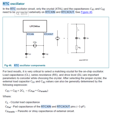
Please refer our recommendation to design your RTC circuit.
DS:
13.5 RTC oscillator
13.5.1 RTC Printed Circuit Board (PCB) design guidelines
RTC Printed Circuit Board (PCB) design guidelines
• Connect the crystal and external load capacitors on the PCB as close as possible to
the oscillator input and output pins of the chip.
• The length of traces in the oscillation circuit should be as short as possible and must
not cross other signal lines.
• Ensure that the load capacitors CX1, CX2, and CX3, in case of third overtone crystal
usage, have a common ground plane.
• Loops must be made as small as possible to minimize the noise coupled in through
the PCB and to keep the parasitics as small as possible.
• Lay out the ground (GND) pattern under crystal unit.
• Do not lay out other signal lines under crystal unit for multi-layered PCB.
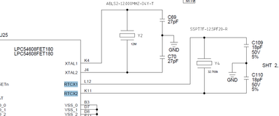
Here is our demo board reference design
Have a nice day
Jun Zhang

