
- Forums
- Product Forums
- General Purpose MicrocontrollersGeneral Purpose Microcontrollers
- i.MX Forumsi.MX Forums
- QorIQ Processing PlatformsQorIQ Processing Platforms
- Identification and SecurityIdentification and Security
- Power ManagementPower Management
- Wireless ConnectivityWireless Connectivity
- RFID / NFCRFID / NFC
- Advanced AnalogAdvanced Analog
- Neural Processing UnitsNeural Processing Units
- MCX Microcontrollers
- S32G
- S32K
- S32V
- MPC5xxx
- Other NXP Products
- S12 / MagniV Microcontrollers
- Powertrain and Electrification Analog Drivers
- Sensors
- Vybrid Processors
- Digital Signal Controllers
- 8-bit Microcontrollers
- ColdFire/68K Microcontrollers and Processors
- PowerQUICC Processors
- OSBDM and TBDML
- S32M
- S32Z/E
-
- Solution Forums
- Software Forums
- MCUXpresso Software and ToolsMCUXpresso Software and Tools
- CodeWarriorCodeWarrior
- MQX Software SolutionsMQX Software Solutions
- Model-Based Design Toolbox (MBDT)Model-Based Design Toolbox (MBDT)
- FreeMASTER
- eIQ Machine Learning Software
- Embedded Software and Tools Clinic
- S32 SDK
- S32 Design Studio
- GUI Guider
- Zephyr Project
- Voice Technology
- Application Software Packs
- Secure Provisioning SDK (SPSDK)
- Processor Expert Software
- Generative AI & LLMs
-
- Topics
- Mobile Robotics - Drones and RoversMobile Robotics - Drones and Rovers
- NXP Training ContentNXP Training Content
- University ProgramsUniversity Programs
- Rapid IoT
- NXP Designs
- SafeAssure-Community
- OSS Security & Maintenance
- Using Our Community
-
- Cloud Lab Forums
-
- Knowledge Bases
- ARM Microcontrollers
- i.MX Processors
- Identification and Security
- Model-Based Design Toolbox (MBDT)
- QorIQ Processing Platforms
- S32 Automotive Processing Platform
- Wireless Connectivity
- CodeWarrior
- MCUXpresso Suite of Software and Tools
- MQX Software Solutions
- RFID / NFC
- Advanced Analog
- Neural Processing Units
-
- NXP Tech Blogs
- Home
- :
- General Purpose Microcontrollers
- :
- LPC Microcontrollers
- :
- Lpc54608 Lqfp208 Emc and Sdram Init
Lpc54608 Lqfp208 Emc and Sdram Init
- Subscribe to RSS Feed
- Mark Topic as New
- Mark Topic as Read
- Float this Topic for Current User
- Bookmark
- Subscribe
- Mute
- Printer Friendly Page

- Mark as New
- Bookmark
- Subscribe
- Mute
- Subscribe to RSS Feed
- Permalink
- Report Inappropriate Content
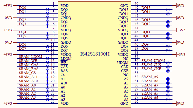
I have my own board includes lpc54608 mcu and IS42S16100H sdram. I referenced sdk example.
SDK_2.3.0_LPCXpresso54608\boards\lpcxpresso54608\driver_examples\emc\sdram.
I am not sure if I made a mistake about hardware. SDRAM_DataBusCheck is ok but SDRAM_AddressBusCheck is not.
I changed _emc_dynamic_timing_config settings according to sdram on board. I am suspicious about %10 hardware and %90 software.
Bank Select Address of IS42S16100H is A11 and there is just one pin because of bank count(2). I directly connected it to A11 on mcu but there is written "The SDRAM bank select pins BA1 and BA0 are connected to address lines A14 and A13, respectively." Does it cause a problem ??
Solved! Go to Solution.

 victorjimenez
- Mark as New
- Bookmark
- Subscribe
- Mute
- Subscribe to RSS Feed
- Permalink
- Report Inappropriate Content
Hello fatih ozen,
Let’s haunt for this problem. You mentioned something that got my attention and it seems that's where the error might be.
A11 pin is IS42's bank select pin. It has no BA0 or BA1 pin. I connected it directly EMC_A11 pin on mcu. This could be my mistake. There is written on page 637 of LPC546xx User Manual (UM10912) "The SDRAM bank select pins BA1 and BA0 are connected to address lines A14 and A13, respectively." Then I soldered A11 pin on sdram to A14 line on mcu and nothing changed. Didn't try A13 line.
As you mentioned in the user manual is stated that BA1 and BA0 are connected to address lines A14 and A13 respectively. In the case of the memory IS42S216100H doesn't have either BA1 or BA0, however A11 is the same as BA0, so you must connect A11 to A13. In the past I've seen several cases where connecting BA1/A11 and BA0 to other pins causes many problems.
Also, I noticed something weird with the code you attached. In the infinite loop that is shown below.
while (1)
{
if (SDRAM_DataBusCheck(sdram) != kStatus_Success) { }
if (SDRAM_AddressBusCheck(sdram, SDRAM_SIZE_BYTES) != kStatus_Success){ }
for (index = 0; index < SDRAM_EXAMPLE_DATALEN; index++)
{
*(uint32_t *)(sdram + index) = index;
}
for (index = 0; index < SDRAM_EXAMPLE_DATALEN; index++)
{
if (*(uint32_t *)(sdram + index) != index)
{
break;
}
}
EMC_Deinit(EMC);
}When you enter the first time to the infinite loop, you make all the process and at the end you call the function EMC_Deinit, so the EMC is not activated anymore after this function. Once you return from the function EMC_Deinit you will start at the beginning of the infinite loop again, but the EMC is not activated anymore so you cannot communicate with the SDRAM. Try to test this functions outside the loop to be sure that this is not the problem you are facing.
Let me know the results to continue with the support.
Hope it helps!
Victor.
-----------------------------------------------------------------------------------------------------------------------
Note: If this post answers your question, please click the Correct Answer button. Thank you!
-----------------------------------------------------------------------------------------------------------------------
victorjimenez
- Mark as New
- Bookmark
- Subscribe
- Mute
- Subscribe to RSS Feed
- Permalink
- Report Inappropriate Content
Hello fatih ozen,
Let’s haunt for this problem. You mentioned something that got my attention and it seems that's where the error might be.
A11 pin is IS42's bank select pin. It has no BA0 or BA1 pin. I connected it directly EMC_A11 pin on mcu. This could be my mistake. There is written on page 637 of LPC546xx User Manual (UM10912) "The SDRAM bank select pins BA1 and BA0 are connected to address lines A14 and A13, respectively." Then I soldered A11 pin on sdram to A14 line on mcu and nothing changed. Didn't try A13 line.
As you mentioned in the user manual is stated that BA1 and BA0 are connected to address lines A14 and A13 respectively. In the case of the memory IS42S216100H doesn't have either BA1 or BA0, however A11 is the same as BA0, so you must connect A11 to A13. In the past I've seen several cases where connecting BA1/A11 and BA0 to other pins causes many problems.
Also, I noticed something weird with the code you attached. In the infinite loop that is shown below.
while (1)
{
if (SDRAM_DataBusCheck(sdram) != kStatus_Success) { }
if (SDRAM_AddressBusCheck(sdram, SDRAM_SIZE_BYTES) != kStatus_Success){ }
for (index = 0; index < SDRAM_EXAMPLE_DATALEN; index++)
{
*(uint32_t *)(sdram + index) = index;
}
for (index = 0; index < SDRAM_EXAMPLE_DATALEN; index++)
{
if (*(uint32_t *)(sdram + index) != index)
{
break;
}
}
EMC_Deinit(EMC);
}When you enter the first time to the infinite loop, you make all the process and at the end you call the function EMC_Deinit, so the EMC is not activated anymore after this function. Once you return from the function EMC_Deinit you will start at the beginning of the infinite loop again, but the EMC is not activated anymore so you cannot communicate with the SDRAM. Try to test this functions outside the loop to be sure that this is not the problem you are facing.
Let me know the results to continue with the support.
Hope it helps!
Victor.
-----------------------------------------------------------------------------------------------------------------------
Note: If this post answers your question, please click the Correct Answer button. Thank you!
-----------------------------------------------------------------------------------------------------------------------
- Mark as New
- Bookmark
- Subscribe
- Mute
- Subscribe to RSS Feed
- Permalink
- Report Inappropriate Content
Hello Victor,
Thanks for reply.
I moved lines in infinite loop to outside as you mentioned for EMC_Deinit problem. I tried to do sth there but I missed Emc deinitialization. I connected sdram's A11 pin to mcu's A13 pin. Still unsuccessful situation on my side.
Any other suggestion to achieve my goal ?
victorjimenez
- Mark as New
- Bookmark
- Subscribe
- Mute
- Subscribe to RSS Feed
- Permalink
- Report Inappropriate Content
Hello fatih ozen,
Your distributor sent me your schematics and I noticed two things:
- In the MCU you have pins PIO0_2 and PIO0_3 with a pull-up resistor, may I ask why you add this pull-up to these pins?
- You left PIO0_4 floating, I highly recommend you to add a pull-up resistor in this pin, since this pin along with PIO0_5 and PIO0_6 are for the ISP mode. If you leave PIO0_4 floating you may enter to ISP UART/I2C/SPI mode.
You mentioned before that you don't want application notes for different mcu's. The following application note is specific for the LPC54608. It is important to keep in mind all the recommendations that are listed in that application note, specifically to the recommendations regarding the PCB since you are using your own development board.
Regards,
Victor.
- Mark as New
- Bookmark
- Subscribe
- Mute
- Subscribe to RSS Feed
- Permalink
- Report Inappropriate Content
Thank you Victor, problem is solved by myself.
- Mark as New
- Bookmark
- Subscribe
- Mute
- Subscribe to RSS Feed
- Permalink
- Report Inappropriate Content
SDRAM_TSREX_NSWell, Okay. Now writing what I have done till this moment.
I have LPC54608J512BD208 mcu and IS42S216100H - 7TLI sdram on my custom board (C.B).
I have LPC 546xx Evaluation Board (E.B) includes LPC54608FET180 mcu and MT48LC8M16A2B4-6A XIT sdram.
Sdram on E.Board
Clock Frequency = 167 MHz, 128 Mbits = 16 MByte ( 4 banks, 12 rows, 9 columns ), 4096 rows, 512 columns. 16 bits communication.
Sdram on C.Board
Clock Frequency = 143 MHz, 16 Mbits = 2 MByte ( 2 banks, 11 rows, 8 columns ), 2048 rows, 256 columns, 16 bits communication.
I might make a mistake about connecting sdram to mcu. You can see my sdram connection to mcu. I connected everything according to E.B. A11 pin is IS42's bank select pin. It has no BA0 or BA1 pin. I connected it directly EMC_A11 pin on mcu. This could be my mistake. There is written on page 637 of LPC546xx User Manual (UM10912) "The SDRAM bank select pins BA1 and BA0 are connected to address lines A14 and A13, respectively." Then I soldered A11 pin on sdram to A14 line on mcu and nothing changed. Didn't try A13 line. While these happening pin_mux.c settings are okay.
I didn't change anything on fsl_emc.c file. Just changed something on board.c and emc_sdram.c files.
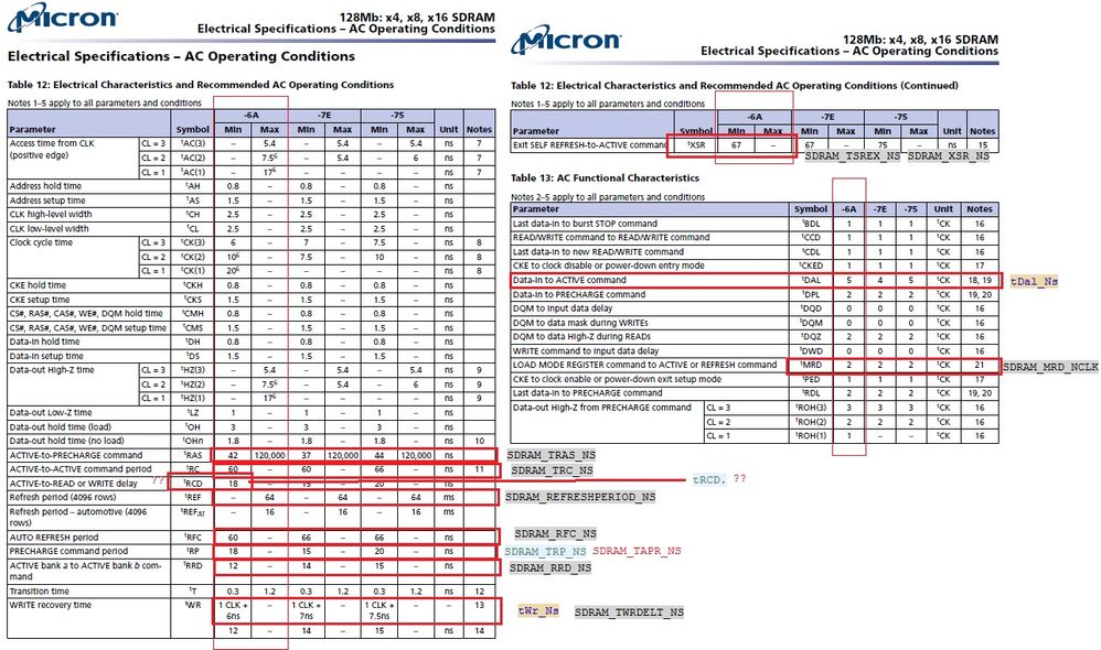
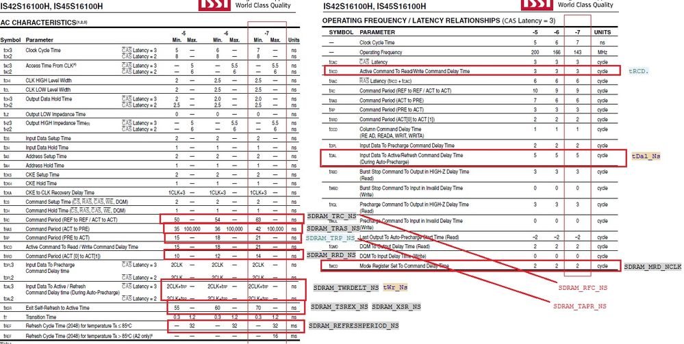
- I could not find "SDRAM_TSREX_NS" in both datasheets but it is similar to SDRAM_XSR_NS. So i defined it same( also the same as E.B.
- I could not find "SDRAM_TAPR_NS" in both datasheets but it is similar to SDRAM_TRP_NS. So i defined it same( also the same as E.B.
- I could make a mistake while defining tWr_Ns and tDal_Ns.
- I could not find "SDRAM_RFC_NS" in IS42's datasheet. Defined it as equals to "SDRAM_TRC_NS".
- SDRAM_RAS_NCLK is defined < Active to read/write delay tRCD.. and tRCD for MT48LC is 18. but it's unit is ns in datasheet. while configuring emc, we need it in nclk. it is 2 for MT48LC. I don't understand that part.
- SDRAM_MODEREG_VALUE is 0x23 for MT48LC. That means
Cas Latency = 2
Burst Type = Sequential
Burst Length = 0,8,8
- I configured SDRAM_MODEREG_VALUE 0x23, 0x33 for IS42S.
Cas Latency = 2 or 3
Burst Type = Sequential
Burst Length = 0,8,8
- I configured SDRAM_DEV_MEMORYMAP 0x01 according to table 656 on page 636 of LPC546xx User Manual (UM10912).
What should I do ? ( Please don't suggest me some application notes for different mcu's. I checked some of them and I searched it on nxp community platform and analyzed some topics.)
How am I checking its truth ? via led on the board. Port 2 Pin 10. If sth went wrong led is turning off. SDRAM_DataBusCheck function works but
in SDRAM_AddressBusCheck it fails.
#include "board.h"
#include "fsl_debug_console.h"
#include "fsl_emc.h"
#include <stdbool.h>
#include "pin_mux.h"
#define SDRAM_BASE_ADDR 0xa0000000
#define SDRAM_SIZE_BYTES (2 * 1024 * 1024)
#define SDRAM_EXAMPLE_DATALEN (SDRAM_SIZE_BYTES / 4)
#define SDRAM_TEST_PATTERN (2)
status_t SDRAM_DataBusCheck(volatile uint32_t *address)
{
uint32_t data = 0;
for (data = 1; data != 0; data <<= 1)
{
*address = data;
if (*address != data)
{
GPIO_PinWrite(GPIO, 2, 10, 0);
return kStatus_Fail;
}
}
return kStatus_Success;
}
status_t SDRAM_AddressBusCheck(volatile uint32_t *address, uint32_t bytes)
{
uint32_t pattern = 0x55555555;
uint32_t size = bytes / 4;
uint32_t offset;
uint32_t checkOffset;
/* write the pattern to the power-of-two address. */
for (offset = 1; offset < size; offset <<= 1)
{
address[offset] = pattern;
}
address[0] = ~pattern;
/* Read and check. */
for (offset = 1; offset < size; offset <<= 1)
{
if (address[offset] != pattern)
{
GPIO_PinWrite(GPIO, 2, 10, 0);
return kStatus_Fail;
}
}
if (address[0] != ~pattern)
{return kStatus_Fail;}
for (offset = 1; offset < size; offset <<= 1)
{
address[offset] = ~pattern;
for (checkOffset = 1; checkOffset < size; checkOffset <<= 1)
{
if ((checkOffset != offset) && (address[checkOffset] != pattern))
{
return kStatus_Fail;
}
}
address[offset] = pattern;
}
return kStatus_Success;
}
void delay(uint32_t a)
{
static uint32_t i = 0;
for (i = 0; i < a; ++i) {__asm("NOP");}
}
int main(void)
{
gpio_pin_config_t led_config = {kGPIO_DigitalOutput, 0,};
uint32_t index;
uint32_t *sdram = (uint32_t *)SDRAM_BASE_ADDR; /* SDRAM start address. */
CLOCK_EnableClock(kCLOCK_InputMux);
CLOCK_AttachClk(BOARD_DEBUG_UART_CLK_ATTACH);
BOARD_InitPins();
BOARD_BootClockFROHF96M();
BOARD_InitDebugConsole();
BOARD_InitSDRAM();
GPIO_PortInit(GPIO, 2);
GPIO_PinInit(GPIO, 2, 10, &led_config);
GPIO_PinWrite(GPIO, 2, 10, 1);
delay(3000000);
while (1){
if (SDRAM_DataBusCheck(sdram) != kStatus_Success) { }
if (SDRAM_AddressBusCheck(sdram, SDRAM_SIZE_BYTES) != kStatus_Success) { }
for (index = 0; index < SDRAM_EXAMPLE_DATALEN; index++) { *(uint32_t *)(sdram + index) = index;}
for (index = 0; index < SDRAM_EXAMPLE_DATALEN; index++) { if (*(uint32_t *)(sdram + index) != index){break;}}
EMC_Deinit(EMC);
}
}
