
- Forums
- Product Forums
- General Purpose MicrocontrollersGeneral Purpose Microcontrollers
- i.MX Forumsi.MX Forums
- QorIQ Processing PlatformsQorIQ Processing Platforms
- Identification and SecurityIdentification and Security
- Power ManagementPower Management
- Wireless ConnectivityWireless Connectivity
- RFID / NFCRFID / NFC
- Advanced AnalogAdvanced Analog
- MCX Microcontrollers
- S32G
- S32K
- S32V
- MPC5xxx
- Other NXP Products
- S12 / MagniV Microcontrollers
- Powertrain and Electrification Analog Drivers
- Sensors
- Vybrid Processors
- Digital Signal Controllers
- 8-bit Microcontrollers
- ColdFire/68K Microcontrollers and Processors
- PowerQUICC Processors
- OSBDM and TBDML
- S32M
- S32Z/E
-
- Solution Forums
- Software Forums
- MCUXpresso Software and ToolsMCUXpresso Software and Tools
- CodeWarriorCodeWarrior
- MQX Software SolutionsMQX Software Solutions
- Model-Based Design Toolbox (MBDT)Model-Based Design Toolbox (MBDT)
- FreeMASTER
- eIQ Machine Learning Software
- Embedded Software and Tools Clinic
- S32 SDK
- S32 Design Studio
- GUI Guider
- Zephyr Project
- Voice Technology
- Application Software Packs
- Secure Provisioning SDK (SPSDK)
- Processor Expert Software
- Generative AI & LLMs
-
- Topics
- Mobile Robotics - Drones and RoversMobile Robotics - Drones and Rovers
- NXP Training ContentNXP Training Content
- University ProgramsUniversity Programs
- Rapid IoT
- NXP Designs
- SafeAssure-Community
- OSS Security & Maintenance
- Using Our Community
-
- Cloud Lab Forums
-
- Knowledge Bases
- ARM Microcontrollers
- i.MX Processors
- Identification and Security
- Model-Based Design Toolbox (MBDT)
- QorIQ Processing Platforms
- S32 Automotive Processing Platform
- Wireless Connectivity
- CodeWarrior
- MCUXpresso Suite of Software and Tools
- MQX Software Solutions
- RFID / NFC
- Advanced Analog
-
- NXP Tech Blogs
- Home
- :
- General Purpose Microcontrollers
- :
- LPC Microcontrollers
- :
- Re: LPC55Sxx FLASH read &&&&& JLINK programming
LPC55Sxx FLASH read && JLINK programming
- Subscribe to RSS Feed
- Mark Topic as New
- Mark Topic as Read
- Float this Topic for Current User
- Bookmark
- Subscribe
- Mute
- Printer Friendly Page
- Mark as New
- Bookmark
- Subscribe
- Mute
- Subscribe to RSS Feed
- Permalink
- Report Inappropriate Content
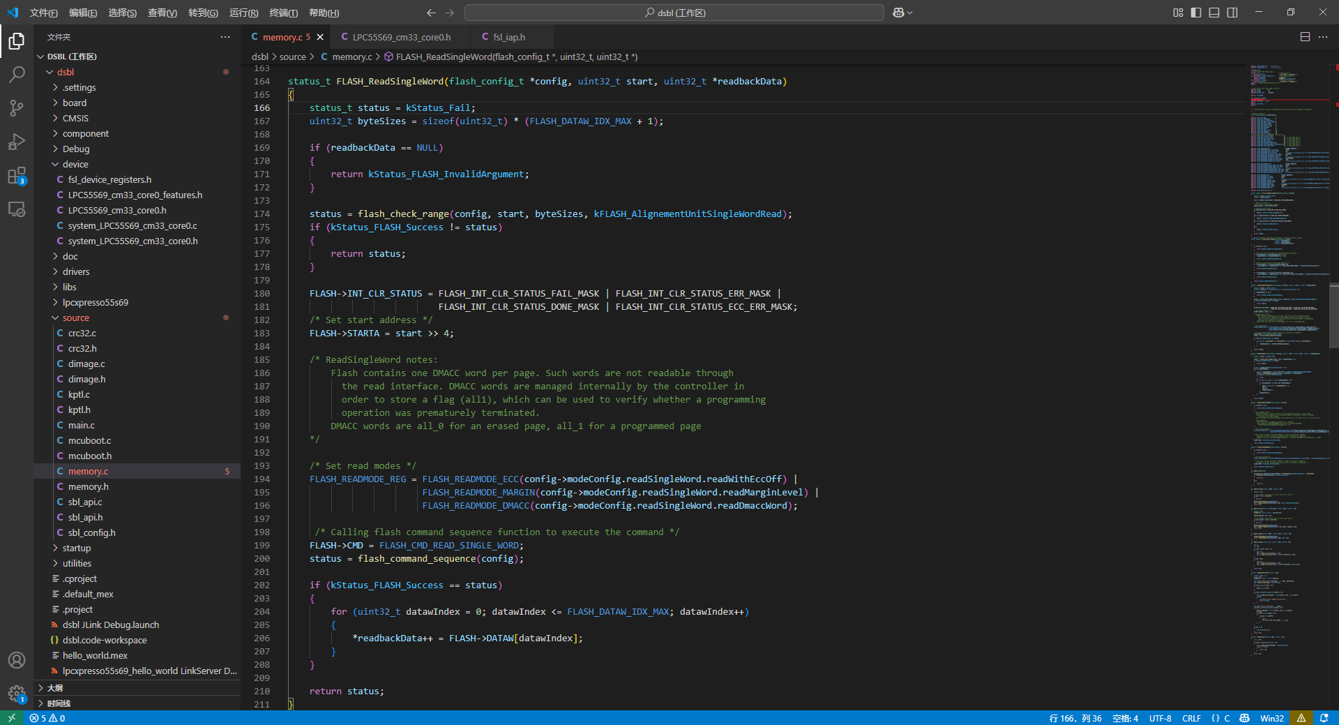
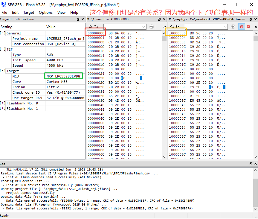
Recently, I have encountered two issues. One is that when the project is in mass production, there are about ten boards. After using JLink to write the firmware onto the LPC5528, when powering on again, there will be a situation where reading a sector with a data size of 256 bytes from the flash will return FLASH->STARTA failure. The development uses Zephyr, and the function is in the position of drivers/flash/soc_flash_mcux.c in the flash_mcux_read() of is_area_readable() and the returned status is FLASH_INT_STATUS_ERR_MASK or FLASH_INT_STATUS_ECC_ERR_MASK. However, I referred to the flash reading operation in the dsbl engineering of LPC55S69, which is consistent with the logic in Zephyr, as shown in the first attached image. But in the document: AN12949 Flash Programming Tips for LPC5500 Series, I also found that there is a flash read operation as shown in the second attached image. So are the final functional effects of these two functions the same? How should I solve this problem? The other issue is that the sample template developed in Zephyr uses LPC55s28, but in fact it is LPC5528. Then in the production bin file and hex file, the offset of the hex file starts from 0x1000 0000. When I use the bin file and download it starting from 0x0, it is also the same. Is there a difference? I saw in the LPC55S6x/LPC55S2x/LPC552x User manual that 0x1000 0000 is the secure part and 0x0 is the ordinary part. The configuration of j-flash is as shown in the third image. Please help solve this quickly because the project has already started mass production and I'm worried that there will be more defects later. thank you.
Solved! Go to Solution.
- Mark as New
- Bookmark
- Subscribe
- Mute
- Subscribe to RSS Feed
- Permalink
- Report Inappropriate Content
Hello @hskating
Thank you.
- Mark as New
- Bookmark
- Subscribe
- Mute
- Subscribe to RSS Feed
- Permalink
- Report Inappropriate Content
Hello @hskating
If the flash is read after erased but before any write operation, an ECC error will occur. Please verify that the entire read flash range has been written to.
For your second question, in your specific case, if you are using an LPC5528, please program it starting from address 0x0.
BR
Alice
- Mark as New
- Bookmark
- Subscribe
- Mute
- Subscribe to RSS Feed
- Permalink
- Report Inappropriate Content
- Mark as New
- Bookmark
- Subscribe
- Mute
- Subscribe to RSS Feed
- Permalink
- Report Inappropriate Content
Hello @hskating
Thank you.