- Forums
- Product Forums
- General Purpose MicrocontrollersGeneral Purpose Microcontrollers
- i.MX Forumsi.MX Forums
- QorIQ Processing PlatformsQorIQ Processing Platforms
- Identification and SecurityIdentification and Security
- Power ManagementPower Management
- Wireless ConnectivityWireless Connectivity
- RFID / NFCRFID / NFC
- Advanced AnalogAdvanced Analog
- MCX Microcontrollers
- S32G
- S32K
- S32V
- MPC5xxx
- Other NXP Products
- S12 / MagniV Microcontrollers
- Powertrain and Electrification Analog Drivers
- Sensors
- Vybrid Processors
- Digital Signal Controllers
- 8-bit Microcontrollers
- ColdFire/68K Microcontrollers and Processors
- PowerQUICC Processors
- OSBDM and TBDML
- S32M
- S32Z/E
-
- Solution Forums
- Software Forums
- MCUXpresso Software and ToolsMCUXpresso Software and Tools
- CodeWarriorCodeWarrior
- MQX Software SolutionsMQX Software Solutions
- Model-Based Design Toolbox (MBDT)Model-Based Design Toolbox (MBDT)
- FreeMASTER
- eIQ Machine Learning Software
- Embedded Software and Tools Clinic
- S32 SDK
- S32 Design Studio
- GUI Guider
- Zephyr Project
- Voice Technology
- Application Software Packs
- Secure Provisioning SDK (SPSDK)
- Processor Expert Software
- Generative AI & LLMs
-
- Topics
- Mobile Robotics - Drones and RoversMobile Robotics - Drones and Rovers
- NXP Training ContentNXP Training Content
- University ProgramsUniversity Programs
- Rapid IoT
- NXP Designs
- SafeAssure-Community
- OSS Security & Maintenance
- Using Our Community
-
- Cloud Lab Forums
-
- Knowledge Bases
- ARM Microcontrollers
- i.MX Processors
- Identification and Security
- Model-Based Design Toolbox (MBDT)
- QorIQ Processing Platforms
- S32 Automotive Processing Platform
- Wireless Connectivity
- CodeWarrior
- MCUXpresso Suite of Software and Tools
- MQX Software Solutions
- RFID / NFC
- Advanced Analog
-
- NXP Tech Blogs
I'm trying to measure the internal 1V bandgap reference, BIAS_VREF_1V, with the ADC16, and it's coming out as ~0.91V.
I can't find any specifications for the reference in v2.7 of the User Manual, nor v2.5 of the Datasheet.
I've found elsewhere on the forums that "BIAS_VREF_1V is 1.5% accuracy over working voltage and temperature range", so 0.91V seems a bit far off if it's really supposed to be 1.00V.
Is it actually supposed to be 1.00V, or is it actually a 0.90V band-gap reference? What is the nominal voltage that the 1.5% accuracy is centred on?
已解决! 转到解答。
OK, if anyone else is having this problem: the User Manual marks most of the AUX_BIAS register as "reserved, write as zero". This is incorrect; if you write these fields as zero it resets the calibration / trim fields!
If I write the current value + VENABLE, rather than just writing = VENABLE, I now get a 1.0V reading.
Hi,
I suppose that you use LPC553x family.
The Vref_out pin of LPC553x must be connected to a 220nF cap.
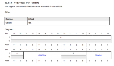
The VREF_OUT pin can output 1.0 to 2.1V DC voltage.
You can write the trim register to adjust the output voltage.
each step in the TRIM2V1 bits is 100mV. For example, the TRIM2V1 is 5, the original voltage is 1V, so the voltage will be 1.0V to 5*100mV=1.5V.
The VREFTRIM is fine turning. Assume it is 5, the voltage will be 5*0.5*1.5mV=3.5mV.
so the voltage will be 1.503V.
Hope it can help you
BR
XiangJun Rong
There's no VREF_OUT pin on the LPC55S69, there's no VREF module (it's called AUX_BIAS, if anything?), and there's no TRIM2V1 or VREFTRIM registers in the SDK anywhere I can find.
Can you point me to the relevant training material, please?
The LPC55S69_cm33_core0.svd does give the AUX_BIAS register ITRIM, PTATITRIM, VREF1VTRIM, VREF1VCURVETRIM, ITRIMCTRL0 and ITRIMCTRL1 subfields, but they definitely don't match the UTRIM register you posted. (AUX_BIAS.VREF1VENABLE would be in the middle of UTRIM.TRIM2V1, if they were the same.)


