- Forums
- Product Forums
- General Purpose MicrocontrollersGeneral Purpose Microcontrollers
- i.MX Forumsi.MX Forums
- QorIQ Processing PlatformsQorIQ Processing Platforms
- Identification and SecurityIdentification and Security
- Power ManagementPower Management
- Wireless ConnectivityWireless Connectivity
- RFID / NFCRFID / NFC
- Advanced AnalogAdvanced Analog
- MCX Microcontrollers
- S32G
- S32K
- S32V
- MPC5xxx
- Other NXP Products
- S12 / MagniV Microcontrollers
- Powertrain and Electrification Analog Drivers
- Sensors
- Vybrid Processors
- Digital Signal Controllers
- 8-bit Microcontrollers
- ColdFire/68K Microcontrollers and Processors
- PowerQUICC Processors
- OSBDM and TBDML
- S32M
- S32Z/E
-
- Solution Forums
- Software Forums
- MCUXpresso Software and ToolsMCUXpresso Software and Tools
- CodeWarriorCodeWarrior
- MQX Software SolutionsMQX Software Solutions
- Model-Based Design Toolbox (MBDT)Model-Based Design Toolbox (MBDT)
- FreeMASTER
- eIQ Machine Learning Software
- Embedded Software and Tools Clinic
- S32 SDK
- S32 Design Studio
- GUI Guider
- Zephyr Project
- Voice Technology
- Application Software Packs
- Secure Provisioning SDK (SPSDK)
- Processor Expert Software
- Generative AI & LLMs
-
- Topics
- Mobile Robotics - Drones and RoversMobile Robotics - Drones and Rovers
- NXP Training ContentNXP Training Content
- University ProgramsUniversity Programs
- Rapid IoT
- NXP Designs
- SafeAssure-Community
- OSS Security & Maintenance
- Using Our Community
-
- Cloud Lab Forums
-
- Knowledge Bases
- ARM Microcontrollers
- i.MX Processors
- Identification and Security
- Model-Based Design Toolbox (MBDT)
- QorIQ Processing Platforms
- S32 Automotive Processing Platform
- Wireless Connectivity
- CodeWarrior
- MCUXpresso Suite of Software and Tools
- MQX Software Solutions
- RFID / NFC
- Advanced Analog
-
- NXP Tech Blogs
- Home
- :
- 汎用マイクロコントローラ
- :
- LPCマイクロコントローラ
- :
- Re: LPC546xx USB_VBUS
LPC546xx USB_VBUS
- RSS フィードを購読する
- トピックを新着としてマーク
- トピックを既読としてマーク
- このトピックを現在のユーザーにフロートします
- ブックマーク
- 購読
- ミュート
- 印刷用ページ
LPC546xx USB_VBUS
- 新着としてマーク
- ブックマーク
- 購読
- ミュート
- RSS フィードを購読する
- ハイライト
- 印刷
- 不適切なコンテンツを報告
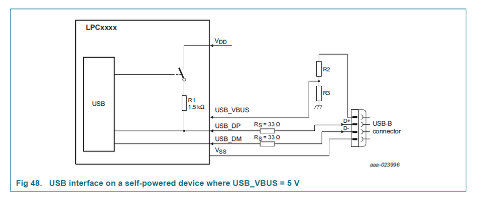
Figure 48 from the LPC546xx datasheet shows the pullup on USB_DP being switched from Vdd. However my understanding is that the USB specification requires this to be connected to USB_VBUS.
Given the problems I have seen with regard to USB device enumeration I suspect that the figure is in fact incorrect and the device does switch to USB_VBUS, but I would appreciate it if someone could confirm this detail. Also, if the minimum working voltage for the USB_VBUS could be provided that would also be very helpful.
Regards,
Padraig
- 新着としてマーク
- ブックマーク
- 購読
- ミュート
- RSS フィードを購読する
- ハイライト
- 印刷
- 不適切なコンテンツを報告
Hi, Padraig,
I have confirmed with AE team, the "Fig 48. USB interface on a self-powered device where USB_VBUS = 5 V" is correct, the USB_DP is pulled up to VDD instead of USB_VBUS with the DCON bit is set in the DEVCMDSTAT register.
Regarding the minimum voltage of the USB_VBUS pin, it is VDD*0.7, if the VDD is 3.3V, it is 0.7*3.3V=2.3V.
Hope it can help you
BR
XiangJun Rong
- 新着としてマーク
- ブックマーク
- 購読
- ミュート
- RSS フィードを購読する
- ハイライト
- 印刷
- 不適切なコンテンツを報告
Thank you for the response.
However, I find the details concerning since I my understanding is that the USB standard requires that USB_DP be pulled up to VBUS and not VDD; or at least that the pull-up should not be attached if VBUS is not present. Can you confirm how this works on the LPCxxx?
Also, from my own testing I can say that USB device enumeration will fail if the voltage on the USB_VBUS pin is below 2.9V. It certainly does not work anywhere close to 2.3V!
- 新着としてマーク
- ブックマーク
- 購読
- ミュート
- RSS フィードを購読する
- ハイライト
- 印刷
- 不適切なコンテンツを報告
Hi, Padraig,
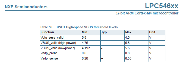
This is the USB_VBUS pin voltage specs in data sheet of LPC546xx, pls refer to it.
Hope it can help you
BR
XiangJun Rong
- 新着としてマーク
- ブックマーク
- 購読
- ミュート
- RSS フィードを購読する
- ハイライト
- 印刷
- 不適切なコンテンツを報告
I had been looking at the datasheet revision 2.6, and it seems this table was added back in Feburary 2020 to revision 2.7; not noticing that was perhaps an oversight on my behalf. In addition to this table it would very useful if the 'Function' listed in the table could be described. I have searched the document and can find no explaination of 'VBUS_valid'. I might guess but I would prefer to have the NXP explain the term as it is intended.
However, and perhaps it is even more important that I note the revision of the datasheet has also changed the title of section 13.7 from "Suggested USB interface solutions" to "Suggested USB0 Full-speed interface solutions". And the table you show above is in a new section "13.8 USB1 High-speed VBUS threshold levels".
So, is it the case that the voltages for USB1 (and given in Table 59) are now different from those previously specified in the datasheet for both USB interfaces?
These new figures do not seem to correspond in any way with the previous description, and I would consider this a very significant alteration of the specification!
Regards,
Padraig

