- Forums
- Product Forums
- General Purpose MicrocontrollersGeneral Purpose Microcontrollers
- i.MX Forumsi.MX Forums
- QorIQ Processing PlatformsQorIQ Processing Platforms
- Identification and SecurityIdentification and Security
- Power ManagementPower Management
- Wireless ConnectivityWireless Connectivity
- RFID / NFCRFID / NFC
- Advanced AnalogAdvanced Analog
- MCX Microcontrollers
- S32G
- S32K
- S32V
- MPC5xxx
- Other NXP Products
- S12 / MagniV Microcontrollers
- Powertrain and Electrification Analog Drivers
- Sensors
- Vybrid Processors
- Digital Signal Controllers
- 8-bit Microcontrollers
- ColdFire/68K Microcontrollers and Processors
- PowerQUICC Processors
- OSBDM and TBDML
- S32M
- S32Z/E
-
- Solution Forums
- Software Forums
- MCUXpresso Software and ToolsMCUXpresso Software and Tools
- CodeWarriorCodeWarrior
- MQX Software SolutionsMQX Software Solutions
- Model-Based Design Toolbox (MBDT)Model-Based Design Toolbox (MBDT)
- FreeMASTER
- eIQ Machine Learning Software
- Embedded Software and Tools Clinic
- S32 SDK
- S32 Design Studio
- GUI Guider
- Zephyr Project
- Voice Technology
- Application Software Packs
- Secure Provisioning SDK (SPSDK)
- Processor Expert Software
- Generative AI & LLMs
-
- Topics
- Mobile Robotics - Drones and RoversMobile Robotics - Drones and Rovers
- NXP Training ContentNXP Training Content
- University ProgramsUniversity Programs
- Rapid IoT
- NXP Designs
- SafeAssure-Community
- OSS Security & Maintenance
- Using Our Community
-
- Cloud Lab Forums
-
- Knowledge Bases
- ARM Microcontrollers
- i.MX Processors
- Identification and Security
- Model-Based Design Toolbox (MBDT)
- QorIQ Processing Platforms
- S32 Automotive Processing Platform
- Wireless Connectivity
- CodeWarrior
- MCUXpresso Suite of Software and Tools
- MQX Software Solutions
- RFID / NFC
- Advanced Analog
-
- NXP Tech Blogs
- Home
- :
- General Purpose Microcontrollers
- :
- LPC Microcontrollers
- :
- LPC54114 erroneous ADC mid range reading from sample app
LPC54114 erroneous ADC mid range reading from sample app
- Subscribe to RSS Feed
- Mark Topic as New
- Mark Topic as Read
- Float this Topic for Current User
- Bookmark
- Subscribe
- Mute
- Printer Friendly Page
LPC54114 erroneous ADC mid range reading from sample app
- Mark as New
- Bookmark
- Subscribe
- Mute
- Subscribe to RSS Feed
- Permalink
- Report Inappropriate Content
LPC54114 SDK ADC Example App displayed mid range (1.65 V = 1/2 of 3.3 V) raw data value is 2178 instead of near 2048, 3 % error
using the NXP OM13089 LPC54114 eval board i ran into a, to me unsolvable, ADC related problem
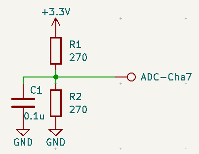
i connected two 270 ohm resistors in series between J8.12 3.3 V and J8.16 GND and a 0.1 uf bypass cap across the resistor connected to GND.
the center tap between the 2 resistors (1.65 V) i connected with a wire to J9.10 ADC0 channel 7. the example apps use ADC channel 7
therefor the supply voltage to this resistor divider is 3.30 V and the center tap at 1.65 V (note the bottom resistor to gnd has a 0.1 uf bypass cap connected across it)
full scale input of 3.3 V should result in a reading of 4096, which it does, as well as 0.0 V input yields a correct reading of 0 V.
however a 1/2 scale input of 1.65 V should result in values near 2048 but in reality it produces 2178 which is a 3.17 % error on a calibrated 12 bit ADC ... this seem TOTALLY UNEXPECTED.
i tried the same 2 example apps (basic and interrupt driven) on a 2nd untouched brand new OM13089 eval board with the same results.
b.t.w. this is not my 1st work related to ADC firmware, but for now i'm stuck and nowhere to go. i used to evaluate the LPC1549 based ADC back in 2014 which is sort of the predecessor to the LPC54114 and had no issues.
further more i tried to lower the ACD clock rate down to 5 MHz and then used the new 54114 setting of the TSAMP sample time at a count of 7.
the question to me is, what is wrong with a NXP factory board using a NXP factory example program to demonstrate the correct operation of the ADC hardware and firmware and get a 3 % mid range error on a 12 bit ADC implementation.
please i need to show some progress with my design and have no idea what i'm doing wrong or what's going on
in anticipation to a solution, a thank you to the NXP support engr.
- Mark as New
- Bookmark
- Subscribe
- Mute
- Subscribe to RSS Feed
- Permalink
- Report Inappropriate Content
to make my ADC channel 7 test hookup visually easier to understand i provide a small schematic clip
given that the two 270 ohm resistors are on Vcc and Gnd on a low impedance source connected, we can see the impedance to the ADC cha 7 as 2 parallel resistors. now we have 135 ohm feeding ADC cha 7.
according to UM10914 rev 2.0, 9 may 2018, NXP user manual the minimum required sample time with up to 200 ohms is 50 ns with a TSAMP of 2.
the cycle time at 80 MHz ADC clock resulting in 12.5 ns x 4.5 is 56.25 ns which should be sufficient by the suggested values in table 522 page 506.
i have also tested the ADC with my own firmware using the NXP SDK config tool for pins and clocks generation with ADC clock rates down to 5 MHz and TSAMP sample delay values up to 7. what i observed were only differences in channel crosstalk, especially with high clock rates and low sample delay times.
however, i NEVER observed any noticeable change in the mid range error of approx 3 % reading higher then the expected value.
i hope that my english description of the problem and my explanation of actions taken and more are understandable.
i deliberately narrowed the issue down to the NXP eval board and untouched NXP provided ADC example code to make a clear point of what's not working right (in my mind). assuming that the example might contain code which shows correct data results using the LPC54114 ADC.
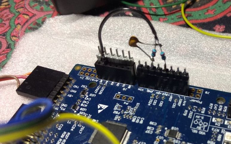
the hookup oft the two 270 ohm resistors to +3.3 V and GND as well as the wire to ADC cha 7 can be seen in the provided pict
the input voltage into the ADC cha 7 was 1.629 V (about 0.6% below 1.65V), Vcc is at 3.280 V (about 0.6 % below 3.3 V).
as can be seen at the table below, 2144 is 2.34 % above the expected value of 2048 ... this can't be an acceptable error on a supposedly calibrated 12 bit ADC mid range value
i would really need help with what either i do wrong with my setup of what's wrong with the setup in general, including setup and scanning the ADC in the NXP example app
ADC clock = 75 MHz TSAMP = 2, ADC clock-div = 1 (+1 = 2, 75 MHz)
[16:03:37:531] ADC interrupt example.
[16:03:47:692] ADC Calibration Done.
[16:03:47:692] Configuration Done.
[16:03:47:692] ADC Full Range: 4096
[16:03:51:662] gAdcResultInfoStruct.result = 2145
[16:03:51:682] gAdcResultInfoStruct.channelNumber = 7
[16:03:51:682] gAdcResultInfoStruct.overrunFlag = 0
[16:03:51:682]
[16:03:52:900] gAdcResultInfoStruct.result = 2140
[16:03:52:900] gAdcResultInfoStruct.channelNumber = 7
[16:03:52:900] gAdcResultInfoStruct.overrunFlag = 0
[16:03:52:927]
[16:03:52:927] gAdcResultInfoStruct.result = 2139
[16:03:52:927] gAdcResultInfoStruct.channelNumber = 7
[16:03:52:927] gAdcResultInfoStruct.overrunFlag = 0
ADC clock = 25 MHz TSAMP = 2, ADC clock-div = 5 (+1 = 6, 25 MHz)
[16:09:21:459] ADC interrupt example.
[16:09:23:668] ADC Calibration Done.
[16:09:23:668] Configuration Done.
[16:09:23:668] ADC Full Range: 4096
[16:09:27:914] gAdcResultInfoStruct.result = 2144
[16:09:27:914] gAdcResultInfoStruct.channelNumber = 7
[16:09:27:914] gAdcResultInfoStruct.overrunFlag = 0
[16:09:27:914]
[16:09:30:198] gAdcResultInfoStruct.result = 2144
[16:09:30:198] gAdcResultInfoStruct.channelNumber = 7
[16:09:30:198] gAdcResultInfoStruct.overrunFlag = 0
- Mark as New
- Bookmark
- Subscribe
- Mute
- Subscribe to RSS Feed
- Permalink
- Report Inappropriate Content
Hi,
I suppose that your resistor divider circuit has issue.
First of all, pls try to remove the capacitor or change the cap from0.1uF to 200pF, the 0.1uF is too large, which leads to large time constant to charge the cap.
Secondly, you use two 270 ohm resistor divider, can you use smaller resistor divider? I suppose that the ADC analog channel has low impedance. If you can not use smaller resistor divider, I suggest you use a analog buffer based on OP amp.
This is the analog RC circuit for ADC channel for the other processor.
The GA0 is analog ADC channel pad, the GA0_RC is the tested voltage source.
Hope it can help you
BR
XiangJun Rong
- Mark as New
- Bookmark
- Subscribe
- Mute
- Subscribe to RSS Feed
- Permalink
- Report Inappropriate Content
disclaimer, i could be wrong, sorry
i don't really understand what u guys do
at fsl_adc_interrupt.c line 74 you set ADC->Ctrl.bit 11 (BYPASSCAL)
"Bypass calibration. Calibration is not utilized. Less time is required when enabling the ADC - particularly following chip power-up. Attempts to launch a calibration cycle are blocked when this bit is set.
. DEMO_ADC_BASE->CTRL |= ADC_CTRL_BYPASSCAL_MASK;
this to me reads that there will be no ADC calibration following this setting ... or i could be wrong ???
as a result i have NOT YET seen that the code after a power up would enter the if () path starting at fsl_adc.c line 302
. /* Launch the calibration cycle or "dummy" conversions. */
. if (ADC_CALIB_CALREQD_MASK == (base->CALIB & ADC_CALIB_CALREQD_MASK))
. {
. /* Calibration is required, do it now. */
. base->CALIB = ADC_CALIB_CALIB_MASK;
which would in my opinion start the cali operation
no, instead the else path at fsl_adc.c line 319 is being executed with starting ADC->Startup.bit 1 (ADC_INIT)
Setting this bit will launch the “dummy” conversion cycle that is required if a calibration is not performed. It will also reload the stored calibration value from a previous calibration unless the BYPASSCAL bit is set.
.else
. {
. /* If a calibration is not performed, launch the conversion cycle. */
. base->STARTUP |= ADC_STARTUP_ADC_INIT_MASK;
/. * A “dummy” conversion cycle requires approximately 6 ADC clocks */
now after all this you return true and print proudly "ADC Calibration Done."
if i'm correct, but i had been wrong before, there has been NEVER any real calibration and NO reload of stored calibration values, but a "ADC Calibration Done" is announced.
maybe i have been too much into banging my head against the real issue but i'm grasping for straws at the moment.
also enabling the calibration which i tried did not fix the real issue of the 3 % off adc results error
sorry, just wanted to point something out which i would consider incorrect.
- Mark as New
- Bookmark
- Subscribe
- Mute
- Subscribe to RSS Feed
- Permalink
- Report Inappropriate Content
Two things in relation to ADCs come to my mind, not sure if it apllies to your problem.
First is the sampling time. The external circuiry on the ADC input must be able to charge/discharge the S&H cap in the configured sampling time (number of ADC clock cycles), or else you get wrong results, which often look like cross-influences between channels.
Second, the ADC power supply. While most MCUs with ADCs have separate AVcc pins, many evaluation boards do connect them directly to Vcc. And often with a reverse battery protection (usually a Shottky diode) to protect the board from certain user mistakes. This will cause a supply current dependant voltage drop in the range you observed.


