- Forums
- Product Forums
- General Purpose MicrocontrollersGeneral Purpose Microcontrollers
- i.MX Forumsi.MX Forums
- QorIQ Processing PlatformsQorIQ Processing Platforms
- Identification and SecurityIdentification and Security
- Power ManagementPower Management
- Wireless ConnectivityWireless Connectivity
- RFID / NFCRFID / NFC
- Advanced AnalogAdvanced Analog
- MCX Microcontrollers
- S32G
- S32K
- S32V
- MPC5xxx
- Other NXP Products
- S12 / MagniV Microcontrollers
- Powertrain and Electrification Analog Drivers
- Sensors
- Vybrid Processors
- Digital Signal Controllers
- 8-bit Microcontrollers
- ColdFire/68K Microcontrollers and Processors
- PowerQUICC Processors
- OSBDM and TBDML
- S32M
- S32Z/E
-
- Solution Forums
- Software Forums
- MCUXpresso Software and ToolsMCUXpresso Software and Tools
- CodeWarriorCodeWarrior
- MQX Software SolutionsMQX Software Solutions
- Model-Based Design Toolbox (MBDT)Model-Based Design Toolbox (MBDT)
- FreeMASTER
- eIQ Machine Learning Software
- Embedded Software and Tools Clinic
- S32 SDK
- S32 Design Studio
- GUI Guider
- Zephyr Project
- Voice Technology
- Application Software Packs
- Secure Provisioning SDK (SPSDK)
- Processor Expert Software
- Generative AI & LLMs
-
- Topics
- Mobile Robotics - Drones and RoversMobile Robotics - Drones and Rovers
- NXP Training ContentNXP Training Content
- University ProgramsUniversity Programs
- Rapid IoT
- NXP Designs
- SafeAssure-Community
- OSS Security & Maintenance
- Using Our Community
-
- Cloud Lab Forums
-
- Knowledge Bases
- ARM Microcontrollers
- i.MX Processors
- Identification and Security
- Model-Based Design Toolbox (MBDT)
- QorIQ Processing Platforms
- S32 Automotive Processing Platform
- Wireless Connectivity
- CodeWarrior
- MCUXpresso Suite of Software and Tools
- MQX Software Solutions
- RFID / NFC
- Advanced Analog
-
- NXP Tech Blogs
- Home
- :
- 汎用マイクロコントローラ
- :
- LPCマイクロコントローラ
- :
- LPC1823JET100 EMC Configuration
LPC1823JET100 EMC Configuration
- RSS フィードを購読する
- トピックを新着としてマーク
- トピックを既読としてマーク
- このトピックを現在のユーザーにフロートします
- ブックマーク
- 購読
- ミュート
- 印刷用ページ
LPC1823JET100 EMC Configuration
- 新着としてマーク
- ブックマーク
- 購読
- ミュート
- RSS フィードを購読する
- ハイライト
- 印刷
- 不適切なコンテンツを報告
I am struggling to understand how to configure the EMC on a LPC1823JET100. I want to use 16-bit data RAM and interface using the byte-lane-select feature ie. 1 data-byte, 1 address-byte, EMC_BLS0 and the other control signals.
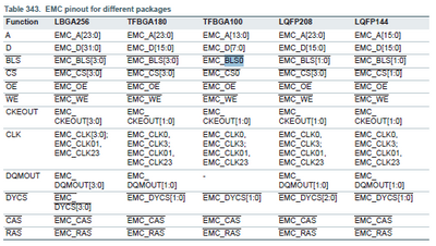
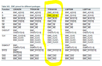
Table 343 from the user guide indicates this should be possible:
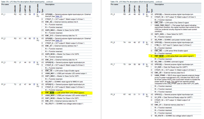
Table 170 in the user guide implies I can use P1_4 or P1_6 for EMC_BLS0.
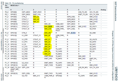
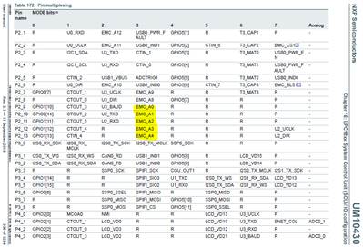
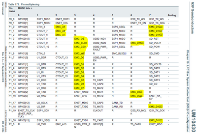
I plan to use P1_7 to P1_14 for EMC_D0 to EMC_D7, P2_9 to P2_13 for EMC_A0 to EMC_A4, and P1_0 to P1_2 for EMC_A5 to EMC_A7. However, table 172 in the user guide implies that setting the mode bits to 3 will set P1_0 to P1_2 to the wrong function, such that I lose EMC_A5 to EMC_A7. I can't find these EMC functions on any other pin for the LPC1823JET100. Is it possible to actively multiplex the function of the P1 bank whilst utilising the EMC interface? Is it actually possible to use implement a 8-bit address, 16-bit data using the LPC1823JET100?
- 新着としてマーク
- ブックマーク
- 購読
- ミュート
- RSS フィードを購読する
- ハイライト
- 印刷
- 不適切なコンテンツを報告
Hi,
Dear Jim Smith,
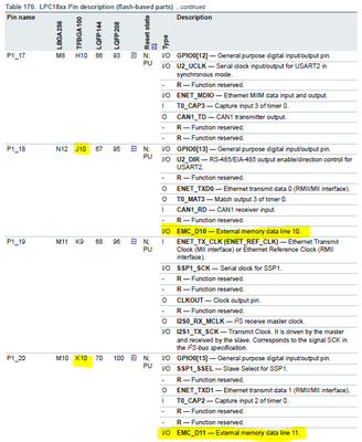
From your description, I see that you want to use 16 bits data width SRAM to EMC, but you would like to access the 16 bits data width SRAM with EMC low 8 bits data bus(EMC_D0~7), you use the P1_0~2 as EMC_A5~A7, I have checked the UM10430.pdf, it appears that EMC_A5~A7 can only route to P1_0~2 as the following Fig.
I think the solution is okay.
This is the connection:
P1_7 to P1_14 for EMC_D0 to EMC_D7
P2_9 to P2_13 for EMC_A0 to EMC_A4
P1_0 to P1_2 for EMC_A5 to EMC_A7; //setting mode=2, the p[in will function as EMC_A5~A7
connect the EMC_OE, EMC_WR, EMC_CSx to the SRAM.
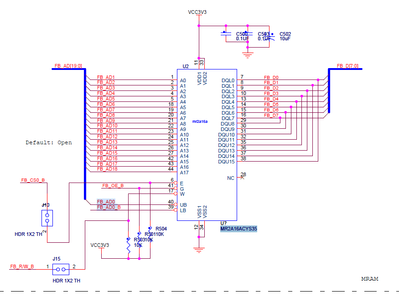
Because you use EMC_D0~7 to SRAM_D0~16, so you have to use EMC_A0 and inverter of EMC_A0 to /LB and /UB of SRAM.
I attach the TWR-MEM, pls refer to MR2A16ACYS35 par circuit.
If I misunderstand you, I am sorry in advance.
- 新着としてマーク
- ブックマーク
- 購読
- ミュート
- RSS フィードを購読する
- ハイライト
- 印刷
- 不適切なコンテンツを報告
Hi xiangjun_rong. Thanks for your response. You're correct about how I intend to connect the address and data, and in the solution you've presented EMC_A0 replaces the function I thought EMC_BLS0 would carry.
I'm still a little confused about the MODE bits. Can these be set separately for each pin in the P1 group? My understanding is that the MODE bits are set for the group, which creates a conflict between EMC_A5~7 and the other EMC signals.
- 新着としてマーク
- ブックマーク
- 購読
- ミュート
- RSS フィードを購読する
- ハイライト
- 印刷
- 不適切なコンテンツを報告
Hi,
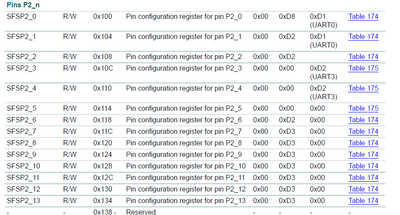
The mode bits can be set separately for each pin rather than the group.
For example,
SFSP2_9 register is Pin configuration register for only pin P2_9.
SFSP2_10 is Pin configuration register for only pin P2_10.
Regarding the question if you use EMC_BLSx or inverter of EMC_A0 to select the data bus, pls check yourself, especially when you access half word address(16 bits data), determine yourself.
BR
XiangJun Rong
- 新着としてマーク
- ブックマーク
- 購読
- ミュート
- RSS フィードを購読する
- ハイライト
- 印刷
- 不適切なコンテンツを報告
Thanks again for your help XiangJun Rong. I wonder if you could clarify something else for me?
Is it possible to use EMCD0~15 on the LPC1823JET100 instead? Tables 170/172 and 343 from the user guide seem to conflict on this. Am I correct to interpret that 16-bit data would inhibit use of an 8-bit address?
- 新着としてマーク
- ブックマーク
- 購読
- ミュート
- RSS フィードを購読する
- ハイライト
- 印刷
- 不適切なコンテンツを報告
Hi, Jim,
I think you have to follow up the Table 343, in other words, you have to use only 8 bits data bus and 14 bits address bus(the SRAM space is 2**14=16K bytes) for the LPC1823JET100 EMC Configuration because of pin limitation. Although there is EMC_D11 pin for the TFBGA100 package, I suppose you can not get all the high data bus from EMC_D8 to D15, so one pin is useless.
If your external SRAM is 16 bits, it is okay if you use only low 8 bits as data bus or use the connection as the memory tower board has done to switch the high and low bytes.
Hope it can help you
BR
XiangJun Rong
