- Forums
- Product Forums
- General Purpose MicrocontrollersGeneral Purpose Microcontrollers
- i.MX Forumsi.MX Forums
- QorIQ Processing PlatformsQorIQ Processing Platforms
- Identification and SecurityIdentification and Security
- Power ManagementPower Management
- Wireless ConnectivityWireless Connectivity
- RFID / NFCRFID / NFC
- Advanced AnalogAdvanced Analog
- MCX Microcontrollers
- S32G
- S32K
- S32V
- MPC5xxx
- Other NXP Products
- S12 / MagniV Microcontrollers
- Powertrain and Electrification Analog Drivers
- Sensors
- Vybrid Processors
- Digital Signal Controllers
- 8-bit Microcontrollers
- ColdFire/68K Microcontrollers and Processors
- PowerQUICC Processors
- OSBDM and TBDML
- S32M
- S32Z/E
-
- Solution Forums
- Software Forums
- MCUXpresso Software and ToolsMCUXpresso Software and Tools
- CodeWarriorCodeWarrior
- MQX Software SolutionsMQX Software Solutions
- Model-Based Design Toolbox (MBDT)Model-Based Design Toolbox (MBDT)
- FreeMASTER
- eIQ Machine Learning Software
- Embedded Software and Tools Clinic
- S32 SDK
- S32 Design Studio
- GUI Guider
- Zephyr Project
- Voice Technology
- Application Software Packs
- Secure Provisioning SDK (SPSDK)
- Processor Expert Software
- Generative AI & LLMs
-
- Topics
- Mobile Robotics - Drones and RoversMobile Robotics - Drones and Rovers
- NXP Training ContentNXP Training Content
- University ProgramsUniversity Programs
- Rapid IoT
- NXP Designs
- SafeAssure-Community
- OSS Security & Maintenance
- Using Our Community
-
- Cloud Lab Forums
-
- Knowledge Bases
- ARM Microcontrollers
- i.MX Processors
- Identification and Security
- Model-Based Design Toolbox (MBDT)
- QorIQ Processing Platforms
- S32 Automotive Processing Platform
- Wireless Connectivity
- CodeWarrior
- MCUXpresso Suite of Software and Tools
- MQX Software Solutions
- RFID / NFC
- Advanced Analog
-
- NXP Tech Blogs
- Home
- :
- ARM Microcontrollers
- :
- LPCマイクロコントローラ・ナレッジ・ベース
- :
- The LPC804 Programmable Logic Unit (PLU)
The LPC804 Programmable Logic Unit (PLU)
- RSS フィードを購読する
- 新着としてマーク
- 既読としてマーク
- ブックマーク
- 購読
- 印刷用ページ
- 不適切なコンテンツを報告
The LPC804 Programmable Logic Unit (PLU)
The LPC804 Programmable Logic Unit (PLU)
This document is an introduction to the Programmable Logic Unit (PLU) provided for the LPC804 MCU device.
PLU is used to create small combinatorial and/or sequential logic networks including simple state machines. This allows to replace external components like the 74xx series, which are used for the glue logic with the microcontroller and external devices, making simple the PCB and saving design costs.
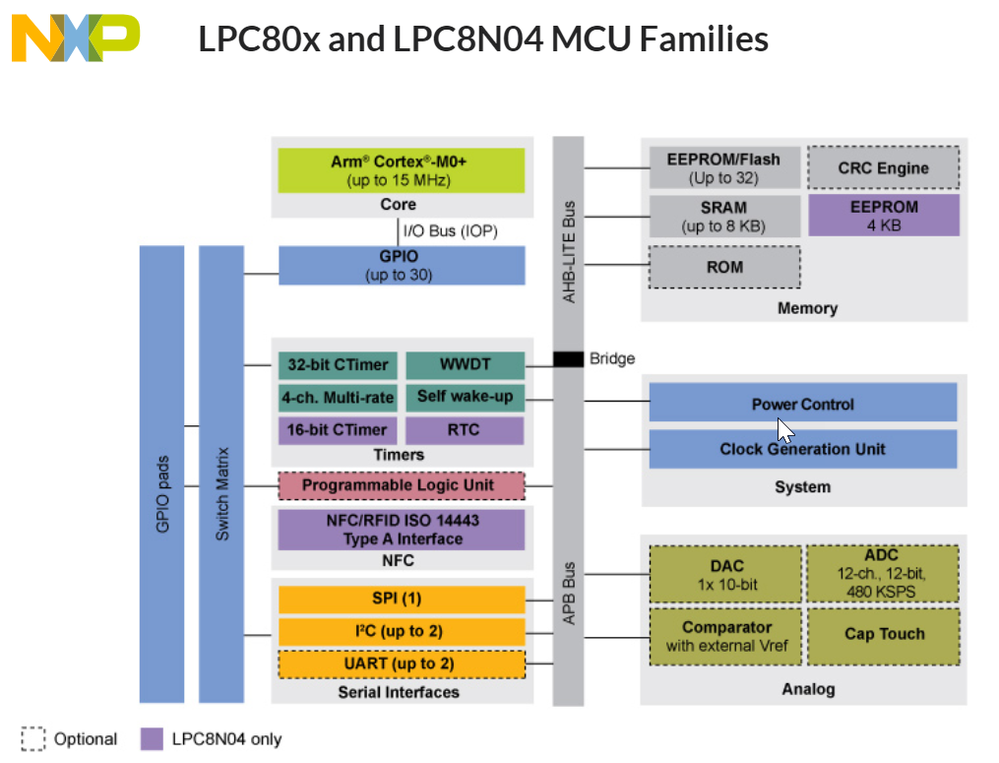
Figure 1. LPC80x MCU families
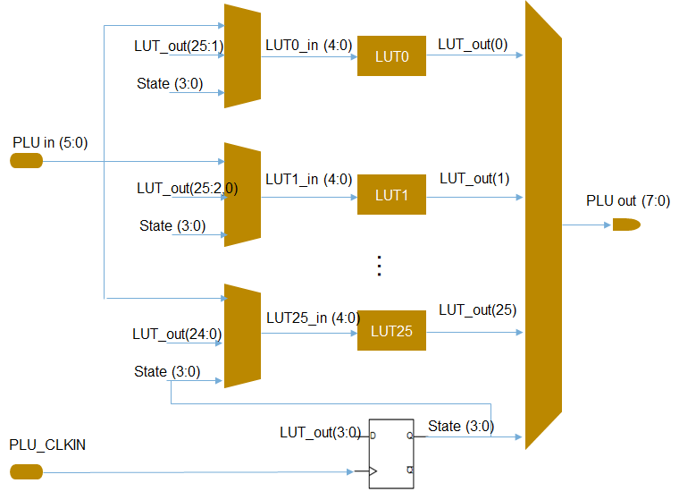
The PLU is comprised of an array of 26 inter-connectable, 5-input Look-up Table (LUT) elements, and 4 flip-flops. Each LUT element contains a 32-bit truth table (look-up table) register and a 32:1 multiplexer. During operation, the five LUT inputs control the select lines of the multiplexer. This structure allows any desired logical combination of the five LUT inputs.
Figure 2. PLU
Features
- The PLU is used to create small combinatorial and/or sequential logic networks including simple state machines.
- The PLU is comprised of an array of 26 inter-connectable, 5-input Look-up Table (LUT) elements, and 4 flip-flops.
- Eight primary outputs can be selected using a multiplexer from among all of the LUT outputs and the 4 flip-flops.
- An external clock to drive the 4 flip-flops must be applied to the PLU_CLKIN pin if a sequential network is implemented.
- Programmable logic can be used to drive on-chip inputs/triggers through external pin-to-pin connections.
- A tool suite is provided to facilitate programming of the PLU to implement the logic network described in a Verilog RTL design.
Advantages
Some advantages of the PLU are:
- Replace the combinational logic of the 7400 series.
- State machine design using Flip-flop.
- Address decoder.
- Pattern match.
- Low-power application. PLU works in deep-sleep and power-down mode.
- Programmable so PLU can be reprogrammed and reused.
- Seamless connection using SWM and PLU.
Pin description
There are up to six primary inputs into the PLU module, one clock input, and eight primary outputs. All the inputs are connected directly to the package pins via chip-level I/O multiplexing. All these pins can be enabled by configuring the relevant SWM register (PINASSIGN_FIXED0).
A particular logic network may not require all of the available inputs or outputs. The user can specify which inputs and outputs to use, and which package pins those inputs and outputs will connect to as part of the overall top-level IO configuration.
Registers
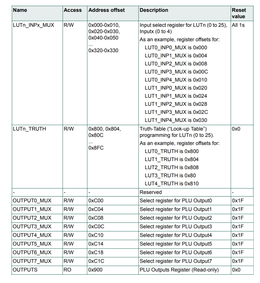
Programming the PLU to implement a particular logic network involves writing to the various Truth Table registers to specify the logic functions to be performed by each of the LUT elements, programming the Input multiplexer registers to select the five inputs presented to each LUT, and programming the Output multiplexer register to select the eight primary outputs from the PLU module.
Programming of all of these registers is performed only during initialization.
Table 1. PLU registers
PLU Shield board with LPCXpresso804
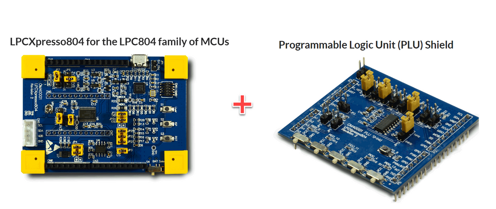
The OM40001 package includes a shield board for use with the LPCXpresso804 board when prototyping programmable logic unit (PLU) designs. The PLU shield provides the following features to assist with this type of development:
- 5 slide switches to enable 5 possible PLU inputs to be connected to VDD (marked as VCC on the Shield) or GND through a resistor (to set those inputs to a logic 1 or zero).
- 8 LEDs with jumpers to connect/disconnect possible PLU outputs for visual status indication.
- Push button option for momentary / edge signal inputs.
- Low-frequency oscillator with 1024Hz and 8Hz outputs.
The PLU shield also includes a test circuit that can be used to implement a simple continuity tester.
Several signals from the LPC804 used on the PLU Shield are shared with other functions on the main LPCXpresso804 board. Please review jumper settings on the LPCXpresso804 board carefully before installing the PLU Shield.
https://www.nxp.com/docs/en/user-guide/UM11083.pdf
Figure 3. LPCXpresso804 + PLU Shield = PLU demo board
PLU input options
On/off switches S1 through S5 connect possible PLU inputs to VDD or GND via a resistor, enabling those inputs to be driven to a known, fixed state. PIO0_8 is connected to a push button (S6) and a 100kohm pull up to VDD; PIO0_8 will be grounded when the button is pressed. Table below shows these connections.
Table 2. PLU input on/off switches.
A digital oscillator circuit is also included on the Shield, with 1.024kHz and 8Hz outputs available. LPC804 signal PIO0_1 can be connected to these oscillator signals in order to provide a low-speed clock to the flip-flops in the PLU block. The center pin (2) of JP12 connects to PIO0_1, so a jumper can be placed onto JP12 to connect this signal to the required clock (see markings on the Shield silk screen.) An external clock can be provided to the PLU by connecting it to the center pin of JP12.
PLU output options
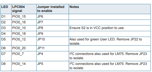
LEDs are used to monitor the PLU outputs. Due to the limited number of pins on the chip/board, some of the inputs and outputs are shared.
Table 3. PLU shield LEDs.
PLU examples
You have two options to find a PLU example:
- Using the SDK for the LPCXpresso804.
You can download the SDK for the LPCXpresso804 from Welcome | MCUXpresso SDK Builder
The PLU project is a simple demonstration program of the SDK PLU driver. In this example, a number of switches are used act as PLU inputs and LEDs are used to monitor the PLU outputs to demonstrate the configuration and use of the Programmable Logic Unit (PLU).
- Using the LPC804 Example Code Bundle.
Code Bundle, containing source code for drivers, example code and project files. You can download it from LPCXpresso804 board for LPC804 Microcontroller (MCU)|NXP
It is recommended to use the PLU configuration tool. Please check the following links for more details.
PLU Tool Direct, LUT-based design: https://www.nxp.com/video/part-2-plu-tool-direct-lut-based-design:Part2-PLU-config-tool-verilog
PLU Tool Schematic design: https://www.nxp.com/video/part-3-plu-tool-schematic-design:Part3-PLU-config-tool-schematic
PLU Tool Importing Verilog files: https://www.nxp.com/video/part-4-plu-tool-importing-verilog-files:Part4-PLU-config-tool-directlut
