- Forums
- Product Forums
- General Purpose MicrocontrollersGeneral Purpose Microcontrollers
- i.MX Forumsi.MX Forums
- QorIQ Processing PlatformsQorIQ Processing Platforms
- Identification and SecurityIdentification and Security
- Power ManagementPower Management
- Wireless ConnectivityWireless Connectivity
- RFID / NFCRFID / NFC
- Advanced AnalogAdvanced Analog
- MCX Microcontrollers
- S32G
- S32K
- S32V
- MPC5xxx
- Other NXP Products
- S12 / MagniV Microcontrollers
- Powertrain and Electrification Analog Drivers
- Sensors
- Vybrid Processors
- Digital Signal Controllers
- 8-bit Microcontrollers
- ColdFire/68K Microcontrollers and Processors
- PowerQUICC Processors
- OSBDM and TBDML
- S32M
- S32Z/E
-
- Solution Forums
- Software Forums
- MCUXpresso Software and ToolsMCUXpresso Software and Tools
- CodeWarriorCodeWarrior
- MQX Software SolutionsMQX Software Solutions
- Model-Based Design Toolbox (MBDT)Model-Based Design Toolbox (MBDT)
- FreeMASTER
- eIQ Machine Learning Software
- Embedded Software and Tools Clinic
- S32 SDK
- S32 Design Studio
- GUI Guider
- Zephyr Project
- Voice Technology
- Application Software Packs
- Secure Provisioning SDK (SPSDK)
- Processor Expert Software
- Generative AI & LLMs
-
- Topics
- Mobile Robotics - Drones and RoversMobile Robotics - Drones and Rovers
- NXP Training ContentNXP Training Content
- University ProgramsUniversity Programs
- Rapid IoT
- NXP Designs
- SafeAssure-Community
- OSS Security & Maintenance
- Using Our Community
-
- Cloud Lab Forums
-
- Knowledge Bases
- ARM Microcontrollers
- i.MX Processors
- Identification and Security
- Model-Based Design Toolbox (MBDT)
- QorIQ Processing Platforms
- S32 Automotive Processing Platform
- Wireless Connectivity
- CodeWarrior
- MCUXpresso Suite of Software and Tools
- MQX Software Solutions
- RFID / NFC
- Advanced Analog
-
- NXP Tech Blogs
- Home
- :
- ARM Microcontrollers
- :
- LPCマイクロコントローラ・ナレッジ・ベース
- :
- Non standard PWM generation using State Configurable Timer (SCT)
Non standard PWM generation using State Configurable Timer (SCT)
- RSS フィードを購読する
- 新着としてマーク
- 既読としてマーク
- ブックマーク
- 購読
- 印刷用ページ
- 不適切なコンテンツを報告
Non standard PWM generation using State Configurable Timer (SCT)
Non standard PWM generation using State Configurable Timer (SCT)
This content was originally contributed to lpcware.com by Dirceu Rodrigues
Introduction
My work evaluating the SCT peripheral with the Hitex LPC4350 board (ARM Cortex-M4/M0) included the generation of non standard PWM signals for use in Power Electronics. At the end, some results would be compared with solutions based on LPC1114 (Cortex-M0), for example. The first idea was to apply a concept that I had used when developing universal controllers for laser printer fuser, at 2001. This is a gate drive for MOSFET / IGBT isolated by pulse transformers.
Two pulses Gate Drive – LPC1114 solution
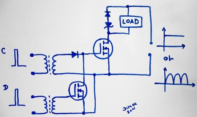
The circuit is implemented with pulse transformers (20 kHz PWM frequency) using the gate-source capacitance as memory. A Schottky diode avoids the stored charge to leak through windings. Thus, it's possible to achieve duty-cycles near to 0 and 100 %, simply applying 1 µs pulses shifted in time - one for charge, other for discharge. A very simplified schematic is shown in Figure 1.
Figure 1. Simplified circuit.
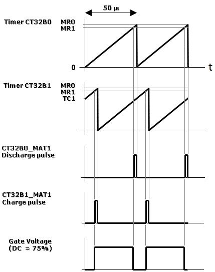
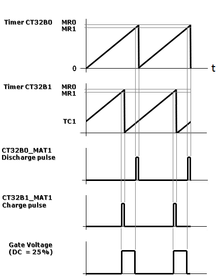
My solution for the LPC1114 - Cortex-M0, uses two timers in a different scheme: Phase-out or lead/lag the counter values. With CT32B0 and CT32B1 32 bit timers, the behavior, including the pulsed outputs, is better understood looking on Figures 2 and 3 for duty-cycles of 75% and 25%. As opposed to common solutions, for each timer, the MR0 and MR1 matching registers values are constant. The difference between them is equivalent to pulse width (1 µs).
The MR0 value also defines the period. The duty-cycle it’s determined through the expression:
DC = TC1 / MR0 (1)
Where, TC1 is the CT32B1 timer value when this one, for the CT32B0, is zero. In order to change the duty-cycle, the code in foreground task establishes a new TC1 and enables the CT32B0 overflow interrupt, where this value is effectively loaded on CT32B1 timer in a safe point (to avoid jitter and other dangerous edges on outputs). Also, the CT32B0 ISR disables itself at the end, ensuring low interrupt overhead. For safety, the first applied pulse is a “discharge pulse”. This solution was proven driving a 930 W (120V/8.7 A) single-phase induction motor and it can be seen in reference [1], using a synchronous AC version of circuit shown in Figure 1 (no diode, four mosfets).
Figure 2. LPC1114 Two Pulses Gate Drive solution - DC 75%.
Figure 3. LPC1114 Two Pulses Gate Drive solution - DC 25%.
Two pulses Gate Drive – LPC4350 SCT solution
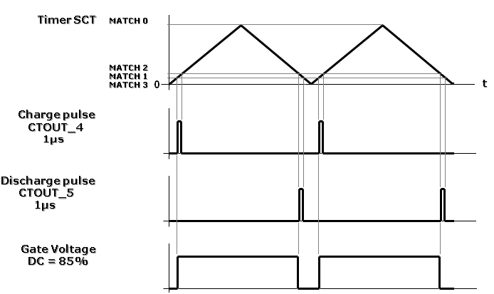
The equivalent SCT implementation for the Two Pulses Gate Driver has the advantage of saving one timer. The pulse generation can be accomplished through a Mealy finite state machine plus the companion SCT counter. The LPC4350 generates 1 µs pulses with repetition rate of 20 kHz on CTOUT_4 and CTOUT_5 outputs. Two pushbuttons allow that a falling edge on CTIN_2 input, start the timer and a low value on CTIN_6, stop it. The counter operates as a unified 32 bit timer (UNIFY = 1) counting up and down (BIDIR = 1). ADC0 input is used to read the voltage on R26 potentiometer. So, the firmware can convert it in PWM change. As for LPC1114, the LPC4350 core and SCT runs in 48 MHz.
Register MATCH 0 defines half-period. The difference between MATCH 2 and MATCH 1 registers is equivalent to pulse width (1 µs). In other words:
PULSE_WIDTH = MATCH 2 - MATCH 1 (2)
Despite this difference be constant, now the MATCH 2 and MATCH 1 contents must change at the same time. Figures 4 and 5 show the waveforms for duty-cycles 15 % and 85 %. For example, the duty-cycle can be determined through the expression:
DC = 1 – (MATCH 1 + 0.5*PULSE_WIDTH )/ MATCH 0 (3)
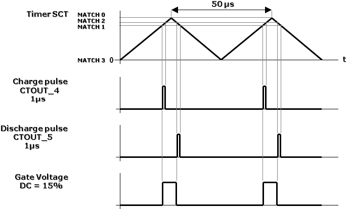
Figure 4. SCT Two Pulses Gate Drive solution - DC 15%.
Note: In companion source code, the PULSE_WIDTH is referred as PULSE_LENGTH.
Figure 5. SCT Two Pulses Gate Drive solution – DC 85%.
In order to achieve this behavior, one simple Finite State Machine with two states has been defined (Table 1):
| STATE | Meaning |
| 0 | CTOUT_4 pulse generation |
| 1 | CTOUT_5 pulse generation |
Table 1. Definition of states.
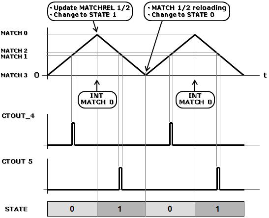
Figure 6 illustrates the relationship between the counter, states and interrupts. The PWM updating scheme takes advantage of following SCT property (as stated on User Manual): “A MATCH register is loaded from the corresponding MATCHREL register when BIDIR is 1 and the counter reaches 0”.
In this application, the ADC0 interrupts MCU in a 24 Hz rate, triggered by TIMER0 MR0 (EM0 rising edge). The code on this ISR determines the new MATCH 1, saves it on global variable match1 and enables the SCT interrupt associated with event “counter reach limit” - in fact, event for MATCH 0. Here note, as stated in expression (3), that DC depends only on MATCH1, since MATCH 0 is constant. The ISR code for MATCH 0 event, updates MATCHREL 1 and MATCHREL 2 registers based on variable match1. Also disables the associated interrupt for low overhead. When counter reaches 0, the MATCH 1, 2 registers will be reloaded from the MATCHREL 1, 2 values automatically. This procedure should avoid jitter and other dangerous edges on outputs.
Note that MATCH registers are never handled by software when counter is running. The new desired values are indirectly loaded on MATCHREL registers. The first values for MATCH registers are intentionally unreachable (> MATCH 0). This ensures that only ADC readings brought useful values to them.
The on board potentiometer generates a voltage from 0 V to 3.3 V, which translates to 0 – 1023 range by the 10 bit AD converter. The MIN_MATCH1 and MAX_MATCH1 predefined values equates to 36 and 1116 (equivalent to duty-cycle 5 % and 95 % DC). Therefore, the software relates ADC0 voltage to with match1 variable approximately through the expression:
match1 = [(MAX_MATCH1 - MIN_MATCH1)*ADC0] / 1024 + (4)
MIN_MATCH1
Note: In the companion source code, the division by 1024 is performed with a 10 bit right shift.
Figure 6. PWM updating scheme - DC 50%.
Table 2 lists the eight states comprising the state machine for the current application. The companion state transition diagram is showed on Figure 7. Here, note other SCT important property, as stated on User’s Manual: “If more than one event associated with the same counter occurs in a given clock cycle, only the state change specified for the highest-numbered event among them takes place”. This applies to events 6 and 7. In normal operation, the event 6 happens periodically in State 1; but when a pushbutton press causes a low level on CTIN_6, the event 7 is fired on State 1 and counter is stopped. The state is driven to 0, with the outputs cleared (until one falling edge on CTIN_2 initiates the counting).
| EVENT ID | Happens in state | Conditions | Actions |
|---|---|---|---|
| 0 | 0 | Falling edge on CTIN_2 | Start counter |
| 1 | 0 | Counter reach MATCH 1 when counting up | Set CTOUT_4 (pulse rise) |
| 2 | 0 | Counter reach MATCH 2 when counting up | Clear CTOUT_4 (pulse fall) |
| 3 | 0 | Counter reach MATCH 0 | Limit counter (defines the half period) Int. to update MATCHREL 1/ 2 Change to STATE 1 |
| 4 | 1 | Counter reach MATCH 2 when counting down | Set CTOUT_5 (pulse rise) |
| 5 | 1 | Counter reach MATCH 1 when counting down | Clear CTOUT_5 (pulse fall) |
| 6 | 1 | Counter reach MATCH 3 (0) | MATCH 1/ 2 automatic reloading Change to STATE 0 |
| 7 | 1 | Counter reach MATCH 3 (0) AND Low value on CTIN_6 | Stop counter MATCH 1/ 2 automatic reloading Change to STATE 0 |
Table 2. Definition of states.
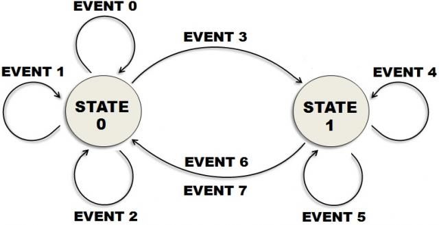
Figure 7. State transition diagram.
Conclusion
The PWM generation carried out by two short pulses shifted in time is a good alternative when isolation and duty-cycles far from 50% are required - specially driving gate charge devices like Mosfet/IGBT. The main advantage over opto-isolated implementations is not necessary create an auxiliary power supply. Regarding to the architecture, the designer can use microcontrollers equipped with UP/DOWN timers (bidirectional), but is required some external glue logic in order to generate those short pulses. In comparison with the LPC1114 presented solution, the SCT version consumes just one timer/counter. As shown, the SCT peripheral is very independent, resulting in low (or no) MCU intervention after an initial configuration.
This simple application used only two inputs, two outputs, two states and eight events. For more complex designs, the SCT provides up to 8 inputs, 16 outputs, 16 events and 32 states. I’ve future plans to make other power electronics applications based on SCT, including a small dot matrix printer controller. Code Red company provides a tool to draw state diagrams and automatically generate code for the SCT engine, called Red State [2] (not used in this application).
Finally, I would like to thank David Donley from NXP, who assisted me by answering my technical enquiries about the State Configurable Timer and suggesting improvements on code.
