- Forums
- Product Forums
- General Purpose MicrocontrollersGeneral Purpose Microcontrollers
- i.MX Forumsi.MX Forums
- QorIQ Processing PlatformsQorIQ Processing Platforms
- Identification and SecurityIdentification and Security
- Power ManagementPower Management
- Wireless ConnectivityWireless Connectivity
- RFID / NFCRFID / NFC
- Advanced AnalogAdvanced Analog
- MCX Microcontrollers
- S32G
- S32K
- S32V
- MPC5xxx
- Other NXP Products
- S12 / MagniV Microcontrollers
- Powertrain and Electrification Analog Drivers
- Sensors
- Vybrid Processors
- Digital Signal Controllers
- 8-bit Microcontrollers
- ColdFire/68K Microcontrollers and Processors
- PowerQUICC Processors
- OSBDM and TBDML
- S32M
- S32Z/E
-
- Solution Forums
- Software Forums
- MCUXpresso Software and ToolsMCUXpresso Software and Tools
- CodeWarriorCodeWarrior
- MQX Software SolutionsMQX Software Solutions
- Model-Based Design Toolbox (MBDT)Model-Based Design Toolbox (MBDT)
- FreeMASTER
- eIQ Machine Learning Software
- Embedded Software and Tools Clinic
- S32 SDK
- S32 Design Studio
- GUI Guider
- Zephyr Project
- Voice Technology
- Application Software Packs
- Secure Provisioning SDK (SPSDK)
- Processor Expert Software
- Generative AI & LLMs
-
- Topics
- Mobile Robotics - Drones and RoversMobile Robotics - Drones and Rovers
- NXP Training ContentNXP Training Content
- University ProgramsUniversity Programs
- Rapid IoT
- NXP Designs
- SafeAssure-Community
- OSS Security & Maintenance
- Using Our Community
-
- Cloud Lab Forums
-
- Knowledge Bases
- ARM Microcontrollers
- i.MX Processors
- Identification and Security
- Model-Based Design Toolbox (MBDT)
- QorIQ Processing Platforms
- S32 Automotive Processing Platform
- Wireless Connectivity
- CodeWarrior
- MCUXpresso Suite of Software and Tools
- MQX Software Solutions
- RFID / NFC
- Advanced Analog
-
- NXP Tech Blogs
- Home
- :
- General Purpose Microcontrollers
- :
- Kinetis Microcontrollers
- :
- Verifying Internal Clocks in Kinetis
Verifying Internal Clocks in Kinetis
- Subscribe to RSS Feed
- Mark Topic as New
- Mark Topic as Read
- Float this Topic for Current User
- Bookmark
- Subscribe
- Mute
- Printer Friendly Page
Verifying Internal Clocks in Kinetis
- Mark as New
- Bookmark
- Subscribe
- Mute
- Subscribe to RSS Feed
- Permalink
- Report Inappropriate Content
Frequently when debugging a board, it's useful to drive the internal clocks of the MCU externally to verify they are at the right frequencies. Here are some tips to do so with the Kinetis family.
Some Kinetis K devices have trace pins available, and these include the TRACE_CLKOUT signal. TRACE_CLKOUT is usually the core/system clock of the system, and is a great option for verifying the CPU clock, or the output of the MCG. Note that the TRACE_CLKOUT signal is always half the core/system clock frequency. Also, the internal trace circuit only drives TRACE_CLKOUT when there is a debug connection. It won't drive if booted without the debugger. It only takes a few lines of code to enable the TRACE_CLKOUT signal, like this:
// Enable TRACE_CLKOUT SIM_SOPT2 |= SIM_SOPT2_TRACECLKSEL_MASK; // Set TRACE_CLKOUT to core/system clock SIM_SCGC5 |= SIM_SCGC5_PORTA_MASK; // Enable PortA clock gate PORTA_PCR6 = PORT_PCR_MUX(0x7) | PORT_PCR_DSE_MASK; // Set pin for TRACE_CLKOUT, high drive strength
Most Kinetis devices do not have the TRACE_CLKOUT signal, so another option is the CLKOUT signal. The CLKOUT signal can have options for which internal clock drives it, including the FlexBus clock (in some older Kinetis derivatives, the only option for this signal was the FlexBus clock, and the signal name was FB_CLKOUT). If your device has the CLKOUT signal, refer to the SIM chapter in the reference manual to see the clock source options for it. Here is some code to enable the FlexBus and the CLKOUT signal:
// Enable CLKOUT, FlexBus Clock SIM_SOPT2 &= ~(0x7 << 5); // Select FlexBus clock for CLKOUT, on Rev2.x silicon SIM_SCGC7 |= SIM_SCGC7_FLEXBUS_MASK; // Enable FlexBus clock gate SIM_SCGC5 |= SIM_SCGC5_PORTC_MASK; // Enable PortC clock gate PORTC_PCR3 = PORT_PCR_MUX(5) | PORT_PCR_DSE_MASK; // Set pin for CLKOUT, high drive strength
But again, not every Kinetis device has the FlexBus or CLKOUT signal. Another option is to use an available PWM channel. The PWM can be configured to run at a frequency half of the timer source clock (usually the peripheral bus clock), and can be configured for a 50% duty cycle. The code below enables a PWM on channel 1 of FTM0 on a Kinetis K device.
// Enable FTM0_CH1 PWM SIM_SCGC5 |= SIM_SCGC5_PORTC_MASK; // Enable PortC clock gate SIM_SCGC6 |= SIM_SCGC6_FTM0_MASK; // Enable FTM0 clock gate PORTC_PCR2 = PORT_PCR_MUX(4) | PORT_PCR_DSE_MASK; // Set pin mux for FTM0 CH1, high drive strength FTM0_MOD = 1; // Set PWM period to 1/2 System clock FTM0_C1SC = FTM_CnSC_MSB_MASK | FTM_CnSC_ELSB_MASK; // Set for edge-aligned PWM FTM0_C1V = 1; // 50% Duty Cycle FTM0_SC = FTM_SC_CLKS(1); // Clock FTM0 from Bus Clock
Kinetis L devices can also use the PWM option shown above, but in Kinetis L the timer peripheral is call TPM instead of FTM, so the register names above need to be changed to TPM.
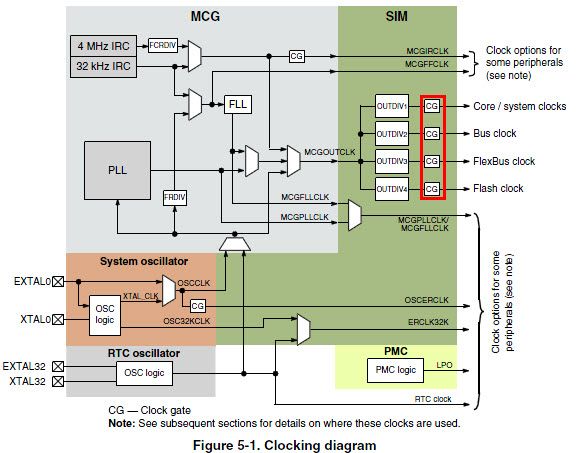
The above options can help verify other clock signals that don't come out directly. It's useful to refer to the clock tree diagram, located in the Clock Distribution chapter of the Kinetis reference manual.
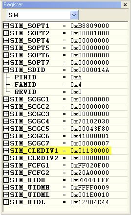
For example, to verify the core clock frequency, and use the PWM method above, the PWM will measure half the peripheral Bus clock frequency. From the diagram above, the Bus clock and core clock are derived from the same clock source, which is the MCGOUTCLK signal, but they have separate clock dividers, boxed in red above. You can use the debugger to verify the clock dividers at run-time.
Attached is a project to show how these clocks can be verified. This example uses a 100MHz K60, but the code can be easily ported to other Kinetis derivatives or toolchains. This project will work on either of the Tower boards TWR-K60N512 or TWR-K60D100M. The startup code uses the PLL to generate MCGOUTCLK of 96MHz. The screenshot of the clock dividers above shows SIM_CLKDIV1 = 0x0113_0000, which means:
- core/system clock divider is 1, or 96MHz
- peripheral Bus clock divider is 2, or 48MHz
- FlexBus clock divider is 2, or 48MHz
- Flash clock divider is 4, or 24MHz
The attached project drives these clock signals out on the pins below. With the Tower system, I like to use the TWR-ELEV cards, and stick some stiff wires into the female headers on the outside of the Primary TWR-ELEV card. Those headers give access to all the signals brought to the edge connectors, and make it easy to measure with a scope.
- TRACE_CLKOUT, PTA6, edge signal A37, 48MHz (core clock / 2)
- CLKOUT, PTC3, edge signal A38, 48MHz (FlexBus clock)
- PWM, PTC2, edge signal A39, 24MHz (peripheral Bus clock / 2)
Original Attachment has been moved to: Clock_Verify.zip
- Mark as New
- Bookmark
- Subscribe
- Mute
- Subscribe to RSS Feed
- Permalink
- Report Inappropriate Content
Hi Derek,
I find this thread is very useful. Thanks.
- Mark as New
- Bookmark
- Subscribe
- Mute
- Subscribe to RSS Feed
- Permalink
- Report Inappropriate Content
For the FRDM-KL05Z there is yet another option. One can use the RTC_CLKOUT on board connector J10 Pin6 = PTB13 to output the 32768 Hz from the crystal oscillator. This requires a configuration of the pin:
ioorh(SIM_SCGC5) = SIM_SCGC5_PORTB_MASK;
PORTB_PCR13 = 0x0300;
ioorb(SIM_SOPT2) = (uint8_t)SIM_SOPT2_RTCCLKOUTSEL_MASK;
These oscillators are sometimes "difficult". For example i found that it may take very long to startup the 32768 Hz crystal oscillator in low power mode. The timeout in the fee_32OSC() sample software may be to short for this to succeed. A good solution was to start the oscillator in high gain mode and then switch to low power mode once it was oscillating.


