- Forums
- Product Forums
- General Purpose MicrocontrollersGeneral Purpose Microcontrollers
- i.MX Forumsi.MX Forums
- QorIQ Processing PlatformsQorIQ Processing Platforms
- Identification and SecurityIdentification and Security
- Power ManagementPower Management
- Wireless ConnectivityWireless Connectivity
- RFID / NFCRFID / NFC
- Advanced AnalogAdvanced Analog
- MCX Microcontrollers
- S32G
- S32K
- S32V
- MPC5xxx
- Other NXP Products
- S12 / MagniV Microcontrollers
- Powertrain and Electrification Analog Drivers
- Sensors
- Vybrid Processors
- Digital Signal Controllers
- 8-bit Microcontrollers
- ColdFire/68K Microcontrollers and Processors
- PowerQUICC Processors
- OSBDM and TBDML
- S32M
- S32Z/E
-
- Solution Forums
- Software Forums
- MCUXpresso Software and ToolsMCUXpresso Software and Tools
- CodeWarriorCodeWarrior
- MQX Software SolutionsMQX Software Solutions
- Model-Based Design Toolbox (MBDT)Model-Based Design Toolbox (MBDT)
- FreeMASTER
- eIQ Machine Learning Software
- Embedded Software and Tools Clinic
- S32 SDK
- S32 Design Studio
- GUI Guider
- Zephyr Project
- Voice Technology
- Application Software Packs
- Secure Provisioning SDK (SPSDK)
- Processor Expert Software
- Generative AI & LLMs
-
- Topics
- Mobile Robotics - Drones and RoversMobile Robotics - Drones and Rovers
- NXP Training ContentNXP Training Content
- University ProgramsUniversity Programs
- Rapid IoT
- NXP Designs
- SafeAssure-Community
- OSS Security & Maintenance
- Using Our Community
-
- Cloud Lab Forums
-
- Knowledge Bases
- ARM Microcontrollers
- i.MX Processors
- Identification and Security
- Model-Based Design Toolbox (MBDT)
- QorIQ Processing Platforms
- S32 Automotive Processing Platform
- Wireless Connectivity
- CodeWarrior
- MCUXpresso Suite of Software and Tools
- MQX Software Solutions
- RFID / NFC
- Advanced Analog
-
- NXP Tech Blogs
- Home
- :
- 汎用マイクロコントローラ
- :
- Kinetisマイクロコントローラ
- :
- Power Sequencing On Kinetis
Power Sequencing On Kinetis
- RSS フィードを購読する
- トピックを新着としてマーク
- トピックを既読としてマーク
- このトピックを現在のユーザーにフロートします
- ブックマーク
- 購読
- ミュート
- 印刷用ページ
Power Sequencing On Kinetis
- 新着としてマーク
- ブックマーク
- 購読
- ミュート
- RSS フィードを購読する
- ハイライト
- 印刷
- 不適切なコンテンツを報告
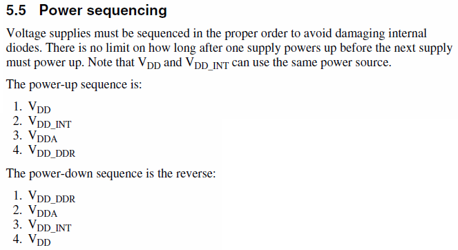
What is the power sequence requirement for Kinetis devices? The K60 data sheet describes a sequence, but it also has conflicting specs for VDD and VDDA. Here is what the K60 data sheet says:
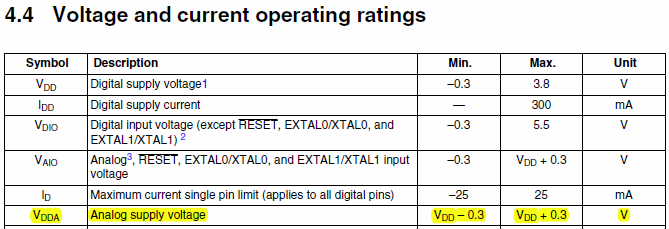
I don't think the following spec is consistent with the power sequence above:
It says that VDDA must be within 0.3V of VDD. The Max spec of VDD + 0.3V makes sense, but not the Min spec, assuming the sequencing spec above is correct. Maybe it should be VSS - 0.3?
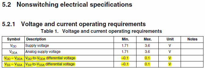
To make things more confusing, it seems there is a conflicting requirement as follows:
Would someone please explain what these specs mean or what they are supposed to be? I have compared the K22 data sheet to the K60, and there isn't a power sequencing section like there is for the K60. But the other specs are the same.
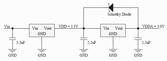
Depending upon the answers to my questions above, my next question might not apply. If I wanted to provide a very low noise supply for VDDA, would the following circuit meet the specs? The Schottky diode will keep VDDA within 0.3V of VDD when Vin is removed. Otherwise VDDA will be follow VDD as it rises, until it reaches its regulation voltage of 3.0V. The LP5907 from TI only costs about 14 cents, and is meant for analog and RF applications.
Another option is a part from Micrel, called a Ripple Blocker. The part number is MIC94300 (MIC94300 - Linear Power Filters - Micrel). It provides >60dB of noise rejection from 40kHz to 5MHz. It is an active device with a voltage drop of about 170 mV. Here is a schematic from the Micrel website:
The MIC94300 is not very expensive. Only about 25 cents or less.
Thanks,
Greg
- 新着としてマーク
- ブックマーク
- 購読
- ミュート
- RSS フィードを購読する
- ハイライト
- 印刷
- 不適切なコンテンツを報告
In the first table VDDA minimum value (VDD -.3) assumes VDD= 0; the figures depicted in that table correspond to the maximum operating conditions whilst the figures depicted in the second table correspond to the normal or typical operating conditions.
- 新着としてマーク
- ブックマーク
- 購読
- ミュート
- RSS フィードを購読する
- ハイライト
- 印刷
- 不適切なコンテンツを報告
Hi Pedro,
Thank you for clarifying the meaning of those tables. In my opinion, Freescale should use the same wording as every other semiconductor company does. The first table should be labeled "Absolute Maximum Ratings", or even "Maximum Ratings". I would have understood right away then. Now it is clear to me, though the tables are in direct contradiction with the power sequencing order. Obviously if the tables are correct then my circuit ideas would not be advised.
Thanks!
Greg


