- Forums
- Product Forums
- General Purpose MicrocontrollersGeneral Purpose Microcontrollers
- i.MX Forumsi.MX Forums
- QorIQ Processing PlatformsQorIQ Processing Platforms
- Identification and SecurityIdentification and Security
- Power ManagementPower Management
- Wireless ConnectivityWireless Connectivity
- RFID / NFCRFID / NFC
- Advanced AnalogAdvanced Analog
- MCX Microcontrollers
- S32G
- S32K
- S32V
- MPC5xxx
- Other NXP Products
- S12 / MagniV Microcontrollers
- Powertrain and Electrification Analog Drivers
- Sensors
- Vybrid Processors
- Digital Signal Controllers
- 8-bit Microcontrollers
- ColdFire/68K Microcontrollers and Processors
- PowerQUICC Processors
- OSBDM and TBDML
- S32M
- S32Z/E
-
- Solution Forums
- Software Forums
- MCUXpresso Software and ToolsMCUXpresso Software and Tools
- CodeWarriorCodeWarrior
- MQX Software SolutionsMQX Software Solutions
- Model-Based Design Toolbox (MBDT)Model-Based Design Toolbox (MBDT)
- FreeMASTER
- eIQ Machine Learning Software
- Embedded Software and Tools Clinic
- S32 SDK
- S32 Design Studio
- GUI Guider
- Zephyr Project
- Voice Technology
- Application Software Packs
- Secure Provisioning SDK (SPSDK)
- Processor Expert Software
- Generative AI & LLMs
-
- Topics
- Mobile Robotics - Drones and RoversMobile Robotics - Drones and Rovers
- NXP Training ContentNXP Training Content
- University ProgramsUniversity Programs
- Rapid IoT
- NXP Designs
- SafeAssure-Community
- OSS Security & Maintenance
- Using Our Community
-
- Cloud Lab Forums
-
- Knowledge Bases
- ARM Microcontrollers
- i.MX Processors
- Identification and Security
- Model-Based Design Toolbox (MBDT)
- QorIQ Processing Platforms
- S32 Automotive Processing Platform
- Wireless Connectivity
- CodeWarrior
- MCUXpresso Suite of Software and Tools
- MQX Software Solutions
- RFID / NFC
- Advanced Analog
-
- NXP Tech Blogs
- Home
- :
- General Purpose Microcontrollers
- :
- Kinetis Microcontrollers
- :
- KL05 SPI Last data bit getting skipped, Whats wrong with the code?
KL05 SPI Last data bit getting skipped, Whats wrong with the code?
- Subscribe to RSS Feed
- Mark Topic as New
- Mark Topic as Read
- Float this Topic for Current User
- Bookmark
- Subscribe
- Mute
- Printer Friendly Page
KL05 SPI Last data bit getting skipped, Whats wrong with the code?
- Mark as New
- Bookmark
- Subscribe
- Mute
- Subscribe to RSS Feed
- Permalink
- Report Inappropriate Content
Hi
I am using codewrrior 10.5. and MKL05Z32VLF4 uc. I am trying to read a register value, the value is not coming proper. The similar code is working fine with K20 board. The expected value from the sensor is 0xB1 (1011 0001) but the value coming is 0x58 (1011 000) Clearly I am missing he last bit. But I don't know how to resolve this issue.
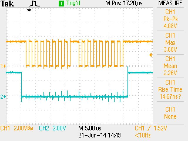
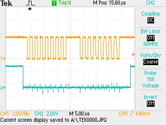
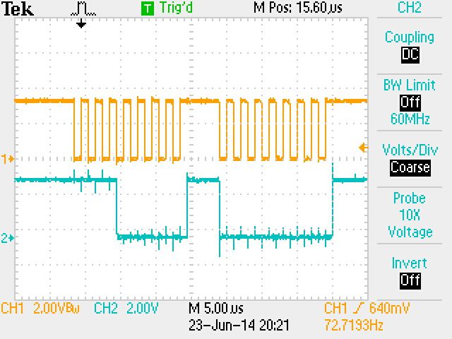
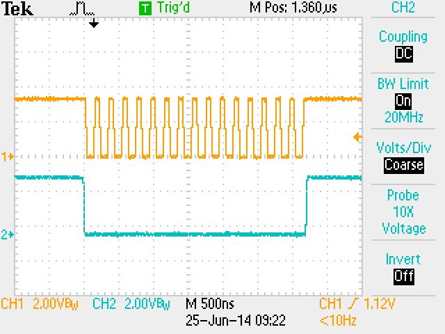
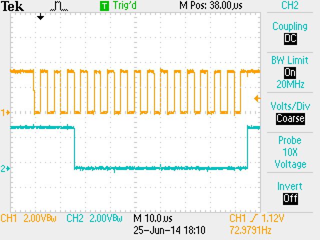
The following image is of SPI_CLK and SPI_SS
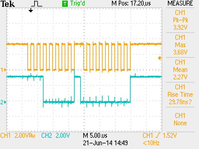
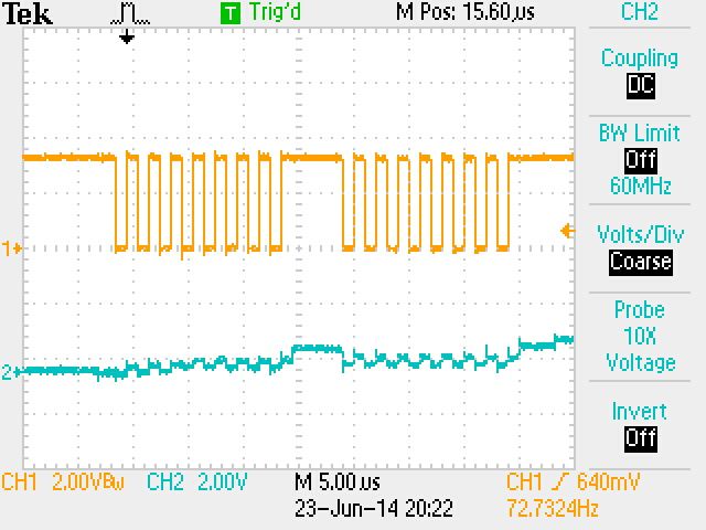
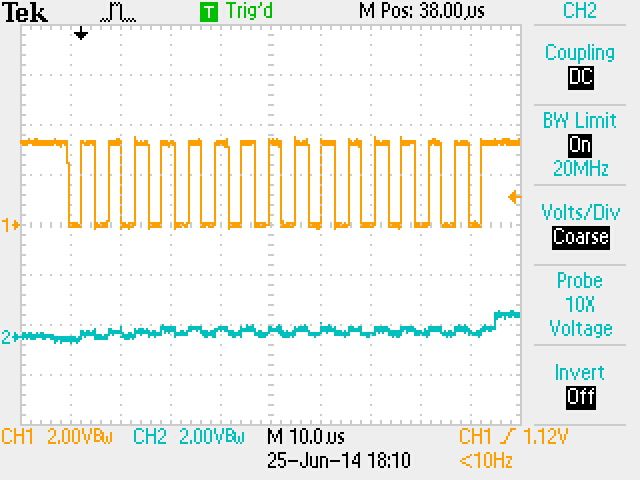
The following image is of SPI_CLK and SPI_MOSI Data being send is 0xE0(read + address) and 0x00 (dummy for receiving data)
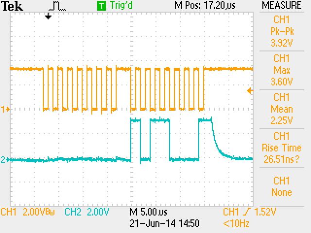
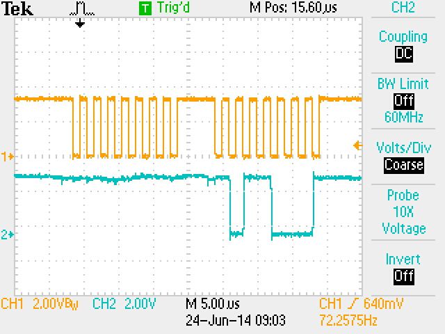
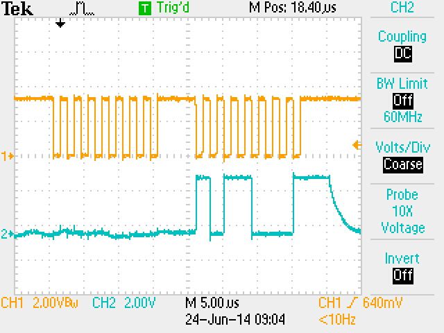
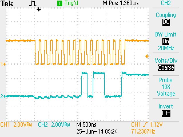
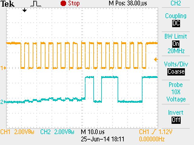
The following image is of SPI_CLK and SPI_MISO the expected value is 0xB1(1011 0001) but in terminal I am getting 0x58(1011 000)
I am attaching the code . Please look into the matter.
Kind Regards
Amit Kumar
Original Attachment has been moved to: KL05-IMU-21-06-2014.zip
- Mark as New
- Bookmark
- Subscribe
- Mute
- Subscribe to RSS Feed
- Permalink
- Report Inappropriate Content
Hi Amit
You have programmed the clock phase incorrectly.
Notice that when your SPI master sends data the data changes on the rising edge of the clock signal.
When your SPI slave device responds with data it is changing the data on the falling edge of the clock.
This means that your SPI master will be reading the slave's data when its clock goes low, which is just 'before' the slave actually drives the new data bit onto the line. The result is that the master is reading one bit too early and the bit data is shifted in the bytes, with the final bit missing.
When using SPI always check the mode that the slave works in from its data sheet and then match the SPI master's settings to it [although some peripherals can match themselves to the setting - SPI flash devices typically can].
Regards
Mark
- Mark as New
- Bookmark
- Subscribe
- Mute
- Subscribe to RSS Feed
- Permalink
- Report Inappropriate Content
Hi Mark
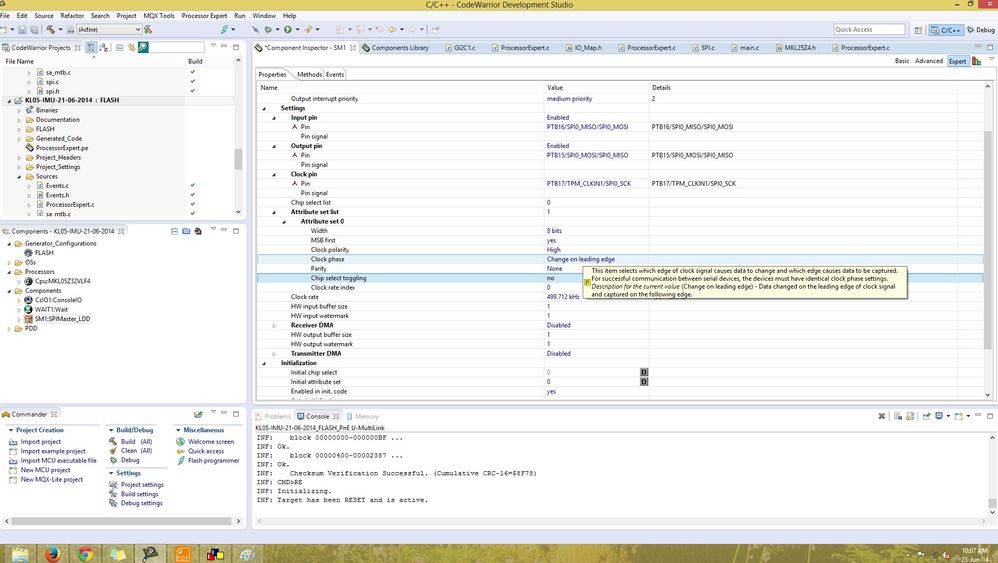
Thanks a lot for the reply. I tried changing the phase from capture on leading edge to change on leading edge. But in that condition it is giving 0x00 as output.
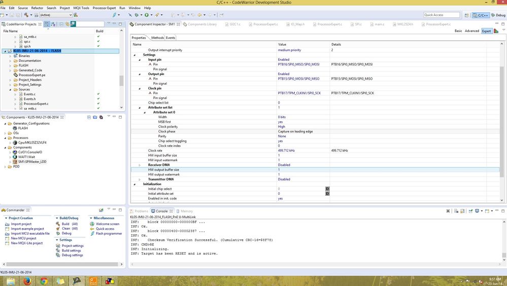
by the following setting I am getting 0x58 as output
If I change the phase, Chip select toggling is also changed to NO. and I am getting 0x00 as output.
How can I change data receive on falling edge?
Thanks and Regards
Amit Kumar
- Mark as New
- Bookmark
- Subscribe
- Mute
- Subscribe to RSS Feed
- Permalink
- Report Inappropriate Content
Amit
What I see from your original code is that the SPI configuration is set up for
/* SPI0_C1: SPIE=0,SPE=0,SPTIE=0,MSTR=1,CPOL=1,CPHA=0,SSOE=1,LSBFE=0 */
SPI0_C1 = (SPI_C1_MSTR_MASK | SPI_C1_CPOL_MASK | SPI_C1_SSOE_MASK); /* Set configuration register */
This is clock phase 0 and clock polarity 1.
There are 4 possibilities for the CPHA and CPOL combination (00, 01, 10 and 11).
Usually the data sheet for the slave device will specify the correct setting but I think that you may need phase 1 and polarity 0 instead.
I would simply overwrite the line that PE generates with the setting and even test all 4 possibilities so that you can see how each looks and also prove which one works correctly.
If you prefer to allow PE to set the bits for you you can still do it afterwards but with the knowledge of what the output should be in case of PE difficulties.
Regards
Mark
- Mark as New
- Bookmark
- Subscribe
- Mute
- Subscribe to RSS Feed
- Permalink
- Report Inappropriate Content
Hi Mark
I tried modifying the generated code from processor expert in the following configurations
1. SPI0_C1 = (SPI_C1_MSTR_MASK | SPI_C1_CPOL_MASK| SPI_C1_CPHA_MASK | SPI_C1_SSOE_MASK); /* Set configuration register */ ,CPOL=1,CPHA=1
2. SPI0_C1 = (SPI_C1_MSTR_MASK | SPI_C1_CPHA_MASK | SPI_C1_SSOE_MASK); /* Set configuration register */ ,CPOL=0,CPHA=1
3. SPI0_C1 = (SPI_C1_MSTR_MASK | SPI_C1_SSOE_MASK); /* Set configuration register */ ,CPOL=0,CPHA=0
I am getting 0x00 as output for these configurations.
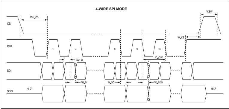
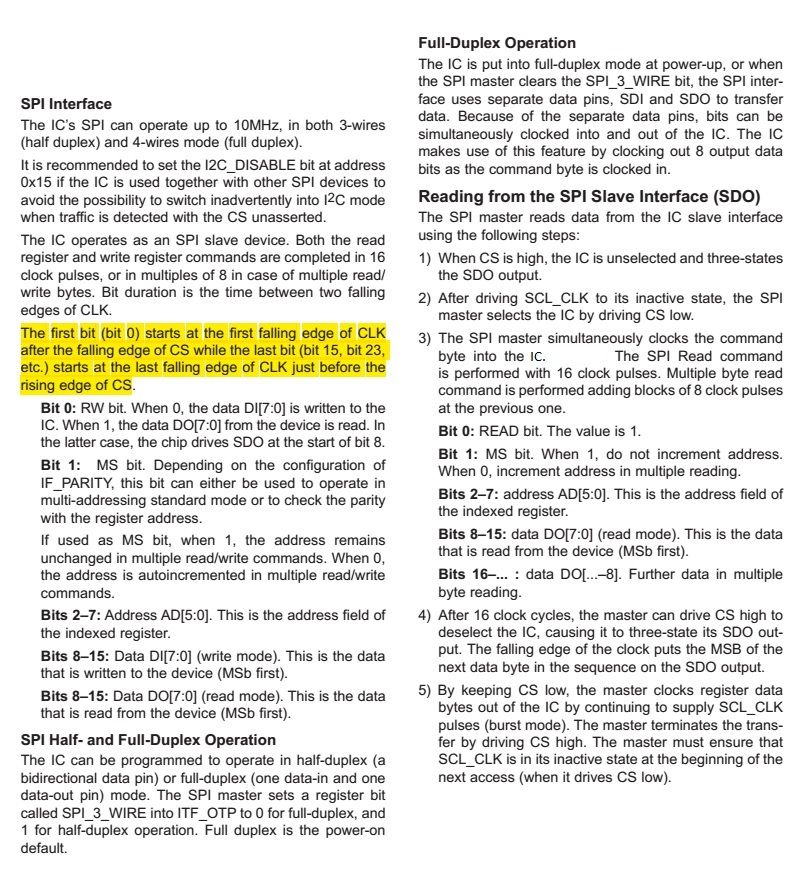
According to the datasheet,
following is the timing diagram
and the SPI configuration details
Kind Regards
Amit Kumar
- Mark as New
- Bookmark
- Subscribe
- Mute
- Subscribe to RSS Feed
- Permalink
- Report Inappropriate Content
Amit
Your device samples on the rising edge and shifts data out on the falling edge. The timing looks like CPOL = '1' and CPHA = '1'.
If you are reading 0x00 it may be that the slave device is not understanding the command that you are sending and so really sending 0x00 back (check the bus again with the oscilloscope). Notice that originally also the timing was wrong for the slave device so it may have also been understanding your transmitted 0xc0 as 0xc1, or 0xe0 and now undestands it as 0xc0 - which could make a difference to its behaviour.
Regards
Mark
- Mark as New
- Bookmark
- Subscribe
- Mute
- Subscribe to RSS Feed
- Permalink
- Report Inappropriate Content
HI Mark
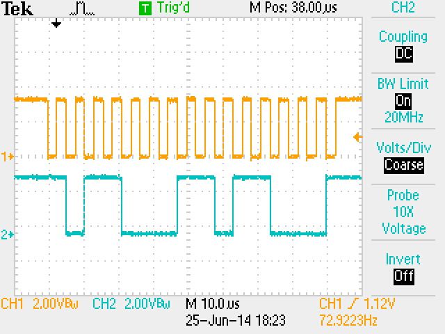
with CPOL = 1, CPHA = 1, following waveforms i got
SCL- SS
SCL-MOSI
SCL-MISO
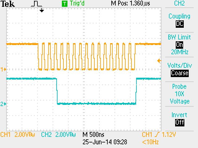
I am wondering can there be an issue of slave select ? as in the 1st fig. the SCL-SS both are not triggering simultaneously. and I used GPIO as ss because I needed 16 bit uninterrupted clk. If I use slave select pin from the component configuration , then after 8 bit there is a break in SS and hence no data is being received.
Kind Regards
Amit Kumar
- Mark as New
- Bookmark
- Subscribe
- Mute
- Subscribe to RSS Feed
- Permalink
- Report Inappropriate Content
Amit
I would enable a pull-up on the SPI_MISO line so that you can better see when the slave is driving the line (driven '0' will be visible.
Normally the slave would always return data when selected but maybe you need to address it as well before it does (?). In any case it looks like the slave is not driving its output (not selected) in your oscilloscope images.
Regards
Mark
- Mark as New
- Bookmark
- Subscribe
- Mute
- Subscribe to RSS Feed
- Permalink
- Report Inappropriate Content
Hi Mark
I connected a pullup on the MISO and got 0xD8 (1101 1000)
When connected pulldown to MISO I am getting the same value 0x58 (0101 1000)
After this I tried manually triggering SS pin, once toggled the SS pin (PTA19) and put it to low logic and the value was coming as 0xB1 which is the required value I did it with 2 registers reading instead of single register reading then it was giving 0xB1 as a constant value for both registers (utter failure). This device worked fine with K20 board. The major diff. was that in K20 I am getting a continuous 16 bit clock in KL05, there is a slight break after 8bit and that's why it is creating this problem. Is there any way to reduce the gap b/w both the clock pulses? If I could do that , I hope my device will start working perfectly.
Thanks & Kind Regards
Amit Kumar
- Mark as New
- Bookmark
- Subscribe
- Mute
- Subscribe to RSS Feed
- Permalink
- Report Inappropriate Content
Amit
Your code is creating the delay:
| while (!(SPI0_S & SPI_S_SPTEF_MASK)); |
SPI0_D = 0xC0 | RegisterAddress;
while (!(SPI0_S & SPI_S_SPRF_MASK)); <-------------------------
i = SPI0_D;
while (!(SPI0_S & SPI_S_SPTEF_MASK));
| SPI0_D = 0x00; | // Dummy byte |
while (!(SPI0_S & SPI_S_SPRF_MASK));
i = SPI0_D;
You can sent the second byte before the first reception is complete (as soon as the Tx has space) and then you should see either no gap between the two, or at least much less.
while (!(SPI0_S & SPI_S_SPTEF_MASK));
SPI0_D = 0xC0 | RegisterAddress;
while (!(SPI0_S & SPI_S_SPTEF_MASK));
SPI0_D = 0x00; // Dummy byte
while (!(SPI0_S & SPI_S_SPRF_MASK));
i = SPI0_D;
while (!(SPI0_S & SPI_S_SPRF_MASK));
i = SPI0_D;
Regards
Mark
- Mark as New
- Bookmark
- Subscribe
- Mute
- Subscribe to RSS Feed
- Permalink
- Report Inappropriate Content
HI Mark
Thanks for the above code. I tried that code , on probing I got the same waveform. I got response from the device support team with respect to the 3 waveforms which I posted initially in this thread. They said:-
"From the diagram you attached, you may mis-configurated the SPI
interface:
MOSI diagram: according to SPI timing diagram in
datasheet, it should be latch data on rising edge of SCLK , but
from your diagram, it changed the state of MOSI when SCLK rising
edge.
MISO diagram: from the diagram, we can read back the data should
be 0xb1 if you read the data on the rising edge, maybe you read
data on the falling edge to cause the read back is 0x58. "
Now what Do you suggest me to do?
I am getting values (0x58) only when CPOL =1 and CPHA =0. In rest all the configuration I am getting 0x00;
Kind Regards
Amit Kumar
- Mark as New
- Bookmark
- Subscribe
- Mute
- Subscribe to RSS Feed
- Permalink
- Report Inappropriate Content
Amit
If the slave is working correctly with the K20 I would do a recording of the signals there to carefully compare with this case.
It is clear that the clock phase was not correct and you you were receiving shifted data as you first showed but it is not clear why changing setting woudl cause the slave to stop responding (or send 0x00). Possibly this careful comparison between teh signals in the two cases may identify a reason.
Regards
Mark
- Mark as New
- Bookmark
- Subscribe
- Mute
- Subscribe to RSS Feed
- Permalink
- Report Inappropriate Content
Hi Mark
I checked the settings in the code generated for K20 uc the init code is as follows
LDD_TDeviceData* SMasterLdd1_Init(LDD_TUserData *UserDataPtr)
{
/* Allocate LDD device structure */
SMasterLdd1_TDeviceDataPtr DeviceDataPrv;
/* {Default RTOS Adapter} Driver memory allocation: Dynamic allocation is simulated by a pointer to the static object */
DeviceDataPrv = &DeviceDataPrv__DEFAULT_RTOS_ALLOC;
DeviceDataPrv->UserData = UserDataPtr; /* Store the RTOS device structure */
/* Interrupt vector(s) allocation */
/* {Default RTOS Adapter} Set interrupt vector: IVT is static, ISR parameter is passed by the global variable */
INT_SPI0__DEFAULT_RTOS_ISRPARAM = DeviceDataPrv;
DeviceDataPrv->TxCommand = 0x80010000U; /* Initialization of current Tx command */
DeviceDataPrv->ErrFlag = 0x00U; /* Clear error flags */
/* Clear the receive counters and pointer */
DeviceDataPrv->InpRecvDataNum = 0x00U; /* Clear the counter of received characters */
DeviceDataPrv->InpDataNumReq = 0x00U; /* Clear the counter of characters to receive by ReceiveBlock() */
DeviceDataPrv->InpDataPtr = NULL; /* Clear the buffer pointer for received characters */
/* Clear the transmit counters and pointer */
DeviceDataPrv->OutSentDataNum = 0x00U; /* Clear the counter of sent characters */
DeviceDataPrv->OutDataNumReq = 0x00U; /* Clear the counter of characters to be send by SendBlock() */
DeviceDataPrv->OutDataPtr = NULL; /* Clear the buffer pointer for data to be transmitted */
/* SIM_SCGC6: SPI0=1 */
SIM_SCGC6 |= SIM_SCGC6_SPI0_MASK;
/* Interrupt vector(s) priority setting */
/* NVICIP12: PRI12=0x80 */
NVICIP12 = NVIC_IP_PRI12(0x80);
/* NVICISER0: SETENA|=0x1000 */
NVICISER0 |= NVIC_ISER_SETENA(0x1000);
/* PORTD_PCR3: ISF=0,MUX=2 */
PORTD_PCR3 = (uint32_t)((PORTD_PCR3 & (uint32_t)~(uint32_t)(
PORT_PCR_ISF_MASK |
PORT_PCR_MUX(0x05)
)) | (uint32_t)(
PORT_PCR_MUX(0x02)
));
/* PORTD_PCR2: ISF=0,MUX=2 */
PORTD_PCR2 = (uint32_t)((PORTD_PCR2 & (uint32_t)~(uint32_t)(
PORT_PCR_ISF_MASK |
PORT_PCR_MUX(0x05)
)) | (uint32_t)(
PORT_PCR_MUX(0x02)
));
/* PORTD_PCR1: ISF=0,MUX=2 */
PORTD_PCR1 = (uint32_t)((PORTD_PCR1 & (uint32_t)~(uint32_t)(
PORT_PCR_ISF_MASK |
PORT_PCR_MUX(0x05)
)) | (uint32_t)(
PORT_PCR_MUX(0x02)
));
/* PORTC_PCR4: ISF=0,MUX=2 */
PORTC_PCR4 = (uint32_t)((PORTC_PCR4 & (uint32_t)~(uint32_t)(
PORT_PCR_ISF_MASK |
PORT_PCR_MUX(0x05)
)) | (uint32_t)(
PORT_PCR_MUX(0x02)
));
/* SPI0_MCR: MSTR=0,CONT_SCKE=0,DCONF=0,FRZ=0,MTFE=0,PCSSE=0,ROOE=1,??=0,??=0,PCSIS=1,DOZE=0,MDIS=0,DIS_TXF=0,DIS_RXF=0,CLR_TXF=0,CLR_RXF=0,SMPL_PT=0,??=0,??=0,??=0,??=0,??=0,??=0,??=0,HALT=1 */
SPI0_MCR = SPI_MCR_DCONF(0x00) |
SPI_MCR_ROOE_MASK |
SPI_MCR_PCSIS(0x01) |
SPI_MCR_SMPL_PT(0x00) |
SPI_MCR_HALT_MASK; /* Set Configuration register */
/* SPI0_MCR: MSTR=1,CONT_SCKE=0,DCONF=0,FRZ=0,MTFE=0,PCSSE=0,ROOE=1,??=0,??=0,PCSIS=1,DOZE=0,MDIS=0,DIS_TXF=1,DIS_RXF=1,CLR_TXF=1,CLR_RXF=1,SMPL_PT=0,??=0,??=0,??=0,??=0,??=0,??=0,??=0,HALT=1 */
SPI0_MCR = SPI_MCR_MSTR_MASK |
SPI_MCR_DCONF(0x00) |
SPI_MCR_ROOE_MASK |
SPI_MCR_PCSIS(0x01) |
SPI_MCR_DIS_TXF_MASK |
SPI_MCR_DIS_RXF_MASK |
SPI_MCR_CLR_TXF_MASK |
SPI_MCR_CLR_RXF_MASK |
SPI_MCR_SMPL_PT(0x00) |
SPI_MCR_HALT_MASK; /* Set Configuration register */
/* SPI0_CTAR0: DBR=1,FMSZ=0x0F,CPOL=1,CPHA=1,LSBFE=0,PCSSCK=0,PASC=0,PDT=2,PBR=2,CSSCK=0,ASC=0,DT=1,BR=1 */
SPI0_CTAR0 = SPI_CTAR_DBR_MASK |
SPI_CTAR_FMSZ(0x0F) |
SPI_CTAR_CPOL_MASK |
SPI_CTAR_CPHA_MASK |
SPI_CTAR_PCSSCK(0x00) |
SPI_CTAR_PASC(0x00) |
SPI_CTAR_PDT(0x02) |
SPI_CTAR_PBR(0x02) |
SPI_CTAR_CSSCK(0x00) |
SPI_CTAR_ASC(0x00) |
SPI_CTAR_DT(0x01) |
SPI_CTAR_BR(0x01); /* Set Clock and Transfer Attributes register */
/* SPI0_SR: TCF=1,TXRXS=0,??=0,EOQF=1,TFUF=1,??=0,TFFF=1,??=0,??=0,??=0,??=1,??=0,RFOF=1,??=0,RFDF=1,??=0,TXCTR=0,TXNXTPTR=0,RXCTR=0,POPNXTPTR=0 */
SPI0_SR = SPI_SR_TCF_MASK |
SPI_SR_EOQF_MASK |
SPI_SR_TFUF_MASK |
SPI_SR_TFFF_MASK |
SPI_SR_RFOF_MASK |
SPI_SR_RFDF_MASK |
SPI_SR_TXCTR(0x00) |
SPI_SR_TXNXTPTR(0x00) |
SPI_SR_RXCTR(0x00) |
SPI_SR_POPNXTPTR(0x00) |
0x00200000U; /* Clear flags */
/* SPI0_RSER: TCF_RE=0,??=0,??=0,EOQF_RE=0,TFUF_RE=0,??=0,TFFF_RE=0,TFFF_DIRS=0,??=0,??=0,??=0,??=0,RFOF_RE=0,??=0,RFDF_RE=1,RFDF_DIRS=0,??=0,??=0,??=0,??=0,??=0,??=0,??=0,??=0,??=0,??=0,??=0,??=0,??=0,??=0,??=0,??=0 */
SPI0_RSER = SPI_RSER_RFDF_RE_MASK; /* Set DMA Interrupt Request Select and Enable register */
/* SPI0_MCR: HALT=0 */
SPI0_MCR &= (uint32_t)~(uint32_t)(SPI_MCR_HALT_MASK);
/* Registration of the device structure */
PE_LDD_RegisterDeviceStructure(PE_LDD_COMPONENT_SMasterLdd1_ID,DeviceDataPrv);
return ((LDD_TDeviceData *)DeviceDataPrv); /* Return pointer to the data data structure */
}
The output waveform from K20 board is :
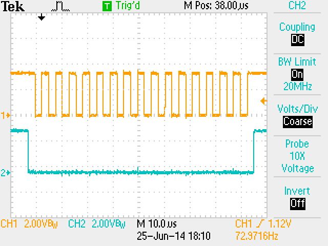
SCL-SS
SCL-MOSI --> 0xE000 (E0-> Read WHO AM I, 00--> Dummy byte for receiving)
SCL-MISO --> 0xB1
Kind Regards
Amit Kumar
- Mark as New
- Bookmark
- Subscribe
- Mute
- Subscribe to RSS Feed
- Permalink
- Report Inappropriate Content
Amit
The K20 code uses CPOL and CPHA = '1' and the waveform confirms that the clocks and bits retunred form the SPI slave are matching in both cases.
This means that I would expect you to read 0x00 (dummy) - 0xb1 in the final case.
Regards
Mark
- Mark as New
- Bookmark
- Subscribe
- Mute
- Subscribe to RSS Feed
- Permalink
- Report Inappropriate Content
HI Mark
I did the following changes in my code for KL05 uc,
CPOL, CPHA = 1
B.R = 187Khz i.e SPI0_BR = SPI_BR_SPPR(0x07) | SPI_BR_SPR(0x03) ;
I modified the read code
unsigned char ReadRegister(unsigned char RegisterAddress)
{
unsigned char i;
while (!(SPI0_S & SPI_S_SPTEF_MASK));
SPI0_D = 0xE0;//0xC0 | RegisterAddress;
while (!(SPI0_S & SPI_S_SPTEF_MASK));
SPI0_D = 0x00; // Dummy byte
while (!(SPI0_S & SPI_S_SPRF_MASK));
i = SPI0_D;
printf("i=0x%02X, \n",i);
return i;
}
SCL-SS
SCL-MOSI
SS-MISO
here At least I managed to get continuous 16 bit clk cycle. I am wondering why the device is not responding the MOSI signal is identical to the earlier signal which I posted for K20 board.
Then I removed the SS pin and left it floating, sometimes the value showed up i.e
SCL-MISO
in this case the value was not being displayed in the terminal window. may be SPIO_D is capturing 16 bit data and since it is an 8 bit register so the 0x00 value is only being stored in it and 0xB1 is getting discarded.
Then I grounded the SS pin and I got the following waveform
SCL-MISO
in this case , in the terminal window 0xB1 is being received.
But the above 2 were the wrong methods. I am wondering why isn't the value being displayed with the correct way. Anyways what are your further suggestion for making it work? Thanks
Kind Regards
Amit Kumar
- Mark as New
- Bookmark
- Subscribe
- Mute
- Subscribe to RSS Feed
- Permalink
- Report Inappropriate Content
Amit
I don't recommend keeping the SS line asserted since it looks like the SPI slave is returning its answer already on the first byte sent (it has probably been queued from a previous access without SS negation).
Also I don't think that the read code is correct since it only reads one of the Rx bytes. The following reads both and returns the second as result:
unsigned char ReadRegister(unsigned char RegisterAddress)
{
unsigned char i, j;
while (!(SPI0_S & SPI_S_SPTEF_MASK));
SPI0_D = 0xE0;//0xC0 | RegisterAddress;
while (!(SPI0_S & SPI_S_SPTEF_MASK)); // wait until the tx buffer can accept a futher byte (this takes place during the first byte transmission)
SPI0_D = 0x00; // Dummy byte - prepare it so that it can be sent without a pause in transmission
while (!(SPI0_S & SPI_S_SPRF_MASK)); // wait until teh first byte has been received
j = SPI0_D; // read first byte (dummy)
while (!(SPI0_S & SPI_S_SPRF_MASK)); // wait until the second byte has been received
i = SPI0_D; // second byte (result)
printf("j=0x%02X, i=0x%02X, \n",j,i);
return i;
}
Regards
Mark
- Mark as New
- Bookmark
- Subscribe
- Mute
- Subscribe to RSS Feed
- Permalink
- Report Inappropriate Content
Hi Mark
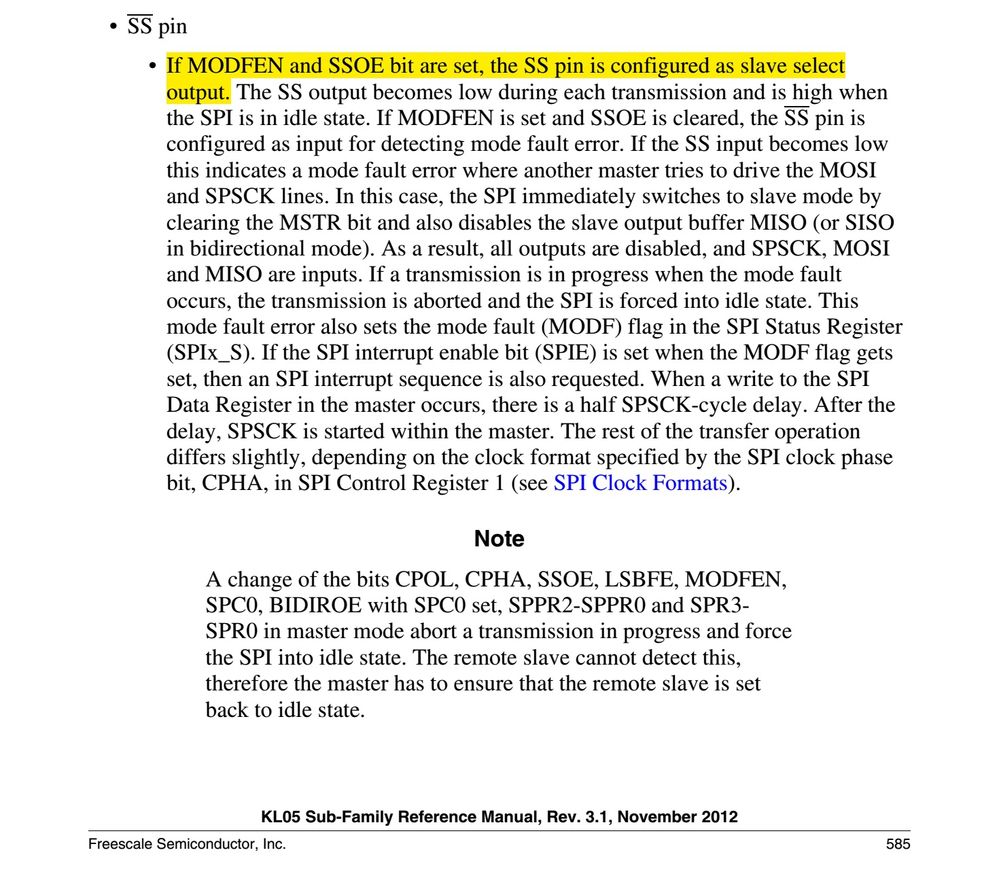
I think may be there is some issue in ss configuration. as in above waveforms if you observe KL05 (16 bit continuous clock) and K20 working waveforms both have identical waveform for SS and MOSI . I Tested with same frequency and it was identical. but I didn't get the MISO waveform back for KL05. When I leave SS pin floating then sometimes I am getting the waveform so these results concludes that the issue may be with SS. I went through the configuration and confirmed that MODFEN, SSOE = 1. What else can be done to make this working? I know it is a dumb ques but it makes me wonder if has anybody had interfaced and tested KL05's SPI. coz I think we have covered and checked almost all the registers settings for SPI, and same device is working fine with K20 so the device dosen't seem to be faulty. KL05 board is also fine as it is generating the required waveforms. So hardware wise it seems to be fine and coding wise I have posted the code and you also went through the codes and all the changes which u told I followed that.
Kind Regards
Amit Kumar
- Mark as New
- Bookmark
- Subscribe
- Mute
- Subscribe to RSS Feed
- Permalink
- Report Inappropriate Content
Amit
It sounds like the problem si more by the SPI slave now.
I would check that the SPI lines (including SS) are in fixed states after powerup/reset and not causing clocks to be detected by the slave, moving it to a different mode so that it then doesn't recognise the addressing when it is sent.
I use the SPI in the KL devices with SPI Flash and SD cards and have not had any problems. There is a workaround to ensure that the SPRF flag operates correctly
https://community.freescale.com/thread/324738
but apart form that no difficultes are known.
If you are controlling the SS line as a GPIO there will be no SS configuration issues in the SPI controller.
Regards
Mark
- Mark as New
- Bookmark
- Subscribe
- Mute
- Subscribe to RSS Feed
- Permalink
- Report Inappropriate Content
Hi Mark
I saw the thread, I moved to codewarrior10.6 from codewarrior 10.5 and tried this code there but the issue remained the same. Also I added
| (volatile unsigned char)SPI0_S; | |
| (volatile unsigned char)SPI0_D; |
and I checked with both SS as GPIO and SS as SPI_SS once at a time.
Kind Regards
Amit Kumar
- Mark as New
- Bookmark
- Subscribe
- Mute
- Subscribe to RSS Feed
- Permalink
- Report Inappropriate Content
Hi Mark
I tried the above code but the result is the same no o/p waveform is being recorded in the oscilloscope. I will try some more things and will update you regarding the condition. Thanks for your support.
Kind Regards
Amit Kumar
