- Forums
- Product Forums
- General Purpose MicrocontrollersGeneral Purpose Microcontrollers
- i.MX Forumsi.MX Forums
- QorIQ Processing PlatformsQorIQ Processing Platforms
- Identification and SecurityIdentification and Security
- Power ManagementPower Management
- Wireless ConnectivityWireless Connectivity
- RFID / NFCRFID / NFC
- Advanced AnalogAdvanced Analog
- MCX Microcontrollers
- S32G
- S32K
- S32V
- MPC5xxx
- Other NXP Products
- S12 / MagniV Microcontrollers
- Powertrain and Electrification Analog Drivers
- Sensors
- Vybrid Processors
- Digital Signal Controllers
- 8-bit Microcontrollers
- ColdFire/68K Microcontrollers and Processors
- PowerQUICC Processors
- OSBDM and TBDML
- S32M
- S32Z/E
-
- Solution Forums
- Software Forums
- MCUXpresso Software and ToolsMCUXpresso Software and Tools
- CodeWarriorCodeWarrior
- MQX Software SolutionsMQX Software Solutions
- Model-Based Design Toolbox (MBDT)Model-Based Design Toolbox (MBDT)
- FreeMASTER
- eIQ Machine Learning Software
- Embedded Software and Tools Clinic
- S32 SDK
- S32 Design Studio
- GUI Guider
- Zephyr Project
- Voice Technology
- Application Software Packs
- Secure Provisioning SDK (SPSDK)
- Processor Expert Software
- Generative AI & LLMs
-
- Topics
- Mobile Robotics - Drones and RoversMobile Robotics - Drones and Rovers
- NXP Training ContentNXP Training Content
- University ProgramsUniversity Programs
- Rapid IoT
- NXP Designs
- SafeAssure-Community
- OSS Security & Maintenance
- Using Our Community
-
- Cloud Lab Forums
-
- Knowledge Bases
- ARM Microcontrollers
- i.MX Processors
- Identification and Security
- Model-Based Design Toolbox (MBDT)
- QorIQ Processing Platforms
- S32 Automotive Processing Platform
- Wireless Connectivity
- CodeWarrior
- MCUXpresso Suite of Software and Tools
- MQX Software Solutions
- RFID / NFC
- Advanced Analog
-
- NXP Tech Blogs
- Home
- :
- 汎用マイクロコントローラ
- :
- Kinetisマイクロコントローラ
- :
- How to flash a kinetis using SWD protocol
How to flash a kinetis using SWD protocol
- RSS フィードを購読する
- トピックを新着としてマーク
- トピックを既読としてマーク
- このトピックを現在のユーザーにフロートします
- ブックマーク
- 購読
- ミュート
- 印刷用ページ
How to flash a kinetis using SWD protocol
- 新着としてマーク
- ブックマーク
- 購読
- ミュート
- RSS フィードを購読する
- ハイライト
- 印刷
- 不適切なコンテンツを報告
Hi,
I am trying to program the flash of MKL05 using SWD (with GPIO).
1. The KL05 Sub-Family Reference Manual, Rev 3.1, November 2012 states at page 139, that AHB-AP is connected to SW-DP. But, from the ARM infocenter I could not find AHB-AP documentation related to Cortex-M0 (Only M1, M3 and M4). Which version of AHB-AP documentation should I refer to?
2. I have succesfully accessed MDM-AP, can read IDR (0x04770031) & Status, and can write/read Control registers. I can also read IDR of AHB-AP. But after writing 0x00000000 to AHB-AP.TAR, the SW-DP.CTRL/STAT shows STICKYERR set (first read of CTRL/STAT after TAR write is 0x00000040, second read of CTRL/STAT after TAR write is 0x00000060). Any AP access after this returns ACK = 4 (fail).
2.5. The AHB-AP.CSW == 0x03000042. Based on Cortex-M1 documentation, bits 27:24 are HPROT[3:0].
Any ideas what is causing this and how to proceed to access Flash Memory Module (FTFA)? Could it be a missing (power) enable somewhere?
BR, -Topi
- 新着としてマーク
- ブックマーク
- 購読
- ミュート
- RSS フィードを購読する
- ハイライト
- 印刷
- 不適切なコンテンツを報告
2. Sorry, the AHB-AP IDR is 0x04770031. MDM-AP IDR is 0x001C0020.
BR, -Topi
- 新着としてマーク
- ブックマーク
- 購読
- ミュート
- RSS フィードを購読する
- ハイライト
- 印刷
- 不適切なコンテンツを報告
Found the problem:
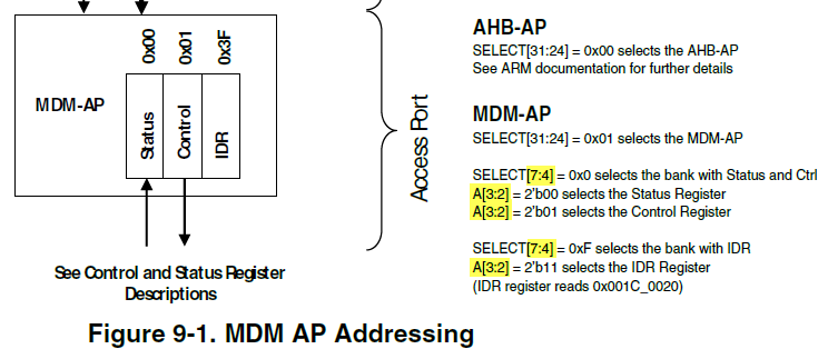
The picture on page 139 of KL05 Sub-Family Reference Manual, Rev. 3.1, November 2012
States that the address range of MDM-AP is 0x00 .. 0x3F.
ARM documentation (MEM-AP) states the address range being 0x00 .. 0xFC (2 LSBs being zero).
I tried to access AHB-AP with address 0x04 (TAR register), but actually it wrote to address 0x10 (BD0), which caused bus error, I guess.
FREESCALE: You should correct the Keystone documentation to express the MDM-AP addresses in the same address format as ARM is doing. Agree?
BR, -Topi
- 新着としてマーク
- ブックマーク
- 購読
- ミュート
- RSS フィードを購読する
- ハイライト
- 印刷
- 不適切なコンテンツを報告
Hello Topi Rinkinen:
Glad to see you found the issue. The addresses in the Reference Manual [0x00/0x01/0x3F] actually refer to the bits SELECT[7:2] as implied by the comments:
So with the 2-bits shift the actual addresses are as you found [0x00/0x04/0xFC]. I agree this can be confusing.
Let me pass your feedback, although the whole range of Kinetis manuals use the same scheme, so this would need a massive update effort.
Regards!
Jorge Gonzalez
- 新着としてマーク
- ブックマーク
- 購読
- ミュート
- RSS フィードを購読する
- ハイライト
- 印刷
- 不適切なコンテンツを報告
Hi,
One more obstacle found..
Flash module (FTFA) registers FTFA_FCCOB[0..B] need to be written during flashing. I struggled a while with a problem that the registers did not read back the written value, but always returned zero.
The solution is to disable COP watchdog in SIM module, right after the reset is released. Then the flashing procedures work as documented.
This information is missing from AN4835. Suggest to update that too.
BR, -Topi
