- Forums
- Product Forums
- General Purpose MicrocontrollersGeneral Purpose Microcontrollers
- i.MX Forumsi.MX Forums
- QorIQ Processing PlatformsQorIQ Processing Platforms
- Identification and SecurityIdentification and Security
- Power ManagementPower Management
- Wireless ConnectivityWireless Connectivity
- RFID / NFCRFID / NFC
- Advanced AnalogAdvanced Analog
- MCX Microcontrollers
- S32G
- S32K
- S32V
- MPC5xxx
- Other NXP Products
- S12 / MagniV Microcontrollers
- Powertrain and Electrification Analog Drivers
- Sensors
- Vybrid Processors
- Digital Signal Controllers
- 8-bit Microcontrollers
- ColdFire/68K Microcontrollers and Processors
- PowerQUICC Processors
- OSBDM and TBDML
- S32M
- S32Z/E
-
- Solution Forums
- Software Forums
- MCUXpresso Software and ToolsMCUXpresso Software and Tools
- CodeWarriorCodeWarrior
- MQX Software SolutionsMQX Software Solutions
- Model-Based Design Toolbox (MBDT)Model-Based Design Toolbox (MBDT)
- FreeMASTER
- eIQ Machine Learning Software
- Embedded Software and Tools Clinic
- S32 SDK
- S32 Design Studio
- GUI Guider
- Zephyr Project
- Voice Technology
- Application Software Packs
- Secure Provisioning SDK (SPSDK)
- Processor Expert Software
- Generative AI & LLMs
-
- Topics
- Mobile Robotics - Drones and RoversMobile Robotics - Drones and Rovers
- NXP Training ContentNXP Training Content
- University ProgramsUniversity Programs
- Rapid IoT
- NXP Designs
- SafeAssure-Community
- OSS Security & Maintenance
- Using Our Community
-
- Cloud Lab Forums
-
- Knowledge Bases
- ARM Microcontrollers
- i.MX Processors
- Identification and Security
- Model-Based Design Toolbox (MBDT)
- QorIQ Processing Platforms
- S32 Automotive Processing Platform
- Wireless Connectivity
- CodeWarrior
- MCUXpresso Suite of Software and Tools
- MQX Software Solutions
- RFID / NFC
- Advanced Analog
-
- NXP Tech Blogs
- Home
- :
- General Purpose Microcontrollers
- :
- Kinetis Microcontrollers
- :
- Re: Hi,Using KE06Z at 5V
Hi,Using KE06Z at 5V
- Subscribe to RSS Feed
- Mark Topic as New
- Mark Topic as Read
- Float this Topic for Current User
- Bookmark
- Subscribe
- Mute
- Printer Friendly Page
Hi,Using KE06Z at 5V
- Mark as New
- Bookmark
- Subscribe
- Mute
- Subscribe to RSS Feed
- Permalink
- Report Inappropriate Content
Hi,
I recently bought the KE06Z dev board. It seems to be powered at 3.3V by default but I really want 5V GPIO's (I picked this board for this capability).
Can anyone advise if the board can be modified to run at 5V? I see in the user's guide there is J14 which switches voltage, but what other modifications would I need to make and is this really advisable? I also note that the IO pin jumpering also takes into account 5V compatibility for some pins (duplicate mappings).
Thanks
- Mark as New
- Bookmark
- Subscribe
- Mute
- Subscribe to RSS Feed
- Permalink
- Report Inappropriate Content
The Freedom KE06Z board can be run at 5 volts, the schematic and user's guide have notes on what has to be changed, which involves changing a couple of jumpers (requires soldering). I have run it at 5 volts. I believe I had to disconnect the accelerometer because I needed the I/O pins that it was attached to and it was clamping the output voltage. Although the CAN transceiver was running on 3.3 volts, I was still able to use it. I do recall populating the SWD connector and using an external BDM to program it, but I believe that was because I had one available and didn't want to use the OpenSDA interface. As far as I know, the OpenSDA will work even if the KE06 is running at 5 volts.
- Mark as New
- Bookmark
- Subscribe
- Mute
- Subscribe to RSS Feed
- Permalink
- Report Inappropriate Content
Yes, I understand that it's possible, I just don't find the information in the UG and schematic to be very clear as to what I should do.
My plan would probably be to solder a header to J14, insert a jumper, and then I would need to remove R76 (0Ω jumper by my reading).
That just leaves the schematic reference, "When 5V for KE06Z, R45, R42, R52, R72 and R74 must be DNP. As these connected pins are not 5V compatible." If I read right, removing those resistors would simply leave the pins completely disconnected. But I could just avoid using (a 5V signal) on those pins?
I will still want to use OpenSDA.
- Mark as New
- Bookmark
- Subscribe
- Mute
- Subscribe to RSS Feed
- Permalink
- Report Inappropriate Content
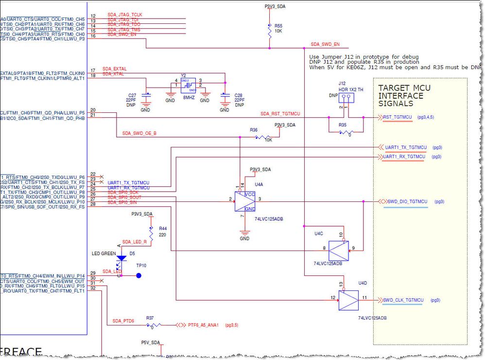
The SWD_DIO_TGTMCU and SWD_CLK_TGTMCU is connect at 74LVC125ADB. From the datasheet of 74LVC125ADB we can know: 5 V tolerant inputs/outputs for interfacing with 5 V logic.
Not sure if you still want to use the UART of OpenSDA. UART1_TX_TGTMCU and UART1_RX_TGTMCU are connect to the PK20DX128VFM5. These two pins can not directly connect to 5V KE06Z.
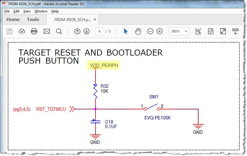
RST_TGTMCU can not directly connect to 5V. But you can use the SW1 reset KE06Z.
Best Regards,
Robin
-----------------------------------------------------------------------------------------------------------------------
Note: If this post answers your question, please click the Correct Answer button. Thank you!
-----------------------------------------------------------------------------------------------------------------------
- Mark as New
- Bookmark
- Subscribe
- Mute
- Subscribe to RSS Feed
- Permalink
- Report Inappropriate Content
Hi Robin
I've removed R52, R45, R42, R72, R74, R76 (J14) and installed a header at J14 that I can jumper for 3.3 or 5V.
I've tested the board at 3.3V and everything seems fine. I even get the debugging console (which I was wrongly expecting to be killed by the cut to the UART TX line).
This leaves me with only 2 questions: Firstly R37 - you can see in your schematic snippet that it goes between the OpenSDA controller and the main MCU, unbuffered. It seems that it's not safe to leave this resistor in place. Can you confirm? I didn't just go ahead and remove it because I wasn't sure what it's function was. I won't test the 5V configuration until I understand if it needs to be removed.
Secondly you say that RST_TGTMCU cannot be connected to the 5V MCU, but as an input pin, this should not matter? Shouldn't retaining R35 still work (even if out of worst case tolerance) because the 5V MCU should still read ~3.3V as a reset high signal?
Thanks
- Mark as New
- Bookmark
- Subscribe
- Mute
- Subscribe to RSS Feed
- Permalink
- Report Inappropriate Content
1.
I don't understand it's function either.
Considering on board OpenSDA(SWD CONNECTOR J7) can be used to debug custom board, I think you can remove R37.
Below information maybe useful for KL26\KL25: If you have a FRDM-KL26Z board and load the mbed debugger (rather than the P&E one) it generates a 32kHz input for the RTC_CLKIN (see SDA_PTD6 and R22). this is useful for preparing SW for designs that later have an external clock generator.
2.
For the RST_TGTMCU(PTA5 KE06), it does not matter connect 3.3V to this Reset_b function pin.
But for the SDA_RST_TGTMCU(PTB1 K20), output pin can't direct connect to 5V. The Kinetis Port pins are only 5V tolerant as inputs. The outputs are not 5V tolerant, and that includes pins configured as open-drain outputs. In output mode, if the pin is pulled above VDD, it will cause the output buffer to drive the output at VDD, which will pull-down the pin voltage to near VDD.
Best Regards,
Robin
-----------------------------------------------------------------------------------------------------------------------
Note: If this post answers your question, please click the Correct Answer button. Thank you!
-----------------------------------------------------------------------------------------------------------------------
- Mark as New
- Bookmark
- Subscribe
- Mute
- Subscribe to RSS Feed
- Permalink
- Report Inappropriate Content
Thanks! I removed R37 and R35 as well. I've successfully tested the board at 5V. Thanks very much for your help.
To be clear, are you saying that an input pull-up at the 5V MCU could cause any K20 open drain output to be pulled up near to 5V?
- Mark as New
- Bookmark
- Subscribe
- Mute
- Subscribe to RSS Feed
- Permalink
- Report Inappropriate Content
The internal pullup at PTA5 of KE06 and the external pullup through R32.
K20 open drain output must not be pulled above VDD(K20).
- Mark as New
- Bookmark
- Subscribe
- Mute
- Subscribe to RSS Feed
- Permalink
- Report Inappropriate Content
Ah yes, thanks very much for the pointers.
- Mark as New
- Bookmark
- Subscribe
- Mute
- Subscribe to RSS Feed
- Permalink
- Report Inappropriate Content
Thanks for the headsup.
It looks like I could remove R35 and put a level shifter across J12, and if I can tack carefully enough, I could also remove R52 (UART1_TX) and R53 (UART1_RX) and patch in level shifters?
It's also been mentioned that the UART1_RX_TGTMCU and RST_TGTMCU lines will probably work even without level shifting (although of course this is outside the worst case margins for level compatibility). Because of the fiddliness of the soldering, I might just leave them directly connected.
Re level shifting, this document is useful: https://www.newark.com/pdfs/techarticles/microchip/3_3vto5vAnalogTipsnTricksBrchr.pdf ; and there is the spare 74HC125 buffer (between TP11 and TP13) that could be used with UART1_TX_TGTMCU in principle? It's curious that the board wasn't already using it for this.

![SIM_SOPT0[RSTPE].jpg SIM_SOPT0[RSTPE].jpg](/t5/image/serverpage/image-id/12041i6ABA341D2E1620CF/image-size/large?v=v2&px=999)
