- Forums
- Product Forums
- General Purpose MicrocontrollersGeneral Purpose Microcontrollers
- i.MX Forumsi.MX Forums
- QorIQ Processing PlatformsQorIQ Processing Platforms
- Identification and SecurityIdentification and Security
- Power ManagementPower Management
- Wireless ConnectivityWireless Connectivity
- RFID / NFCRFID / NFC
- Advanced AnalogAdvanced Analog
- MCX Microcontrollers
- S32G
- S32K
- S32V
- MPC5xxx
- Other NXP Products
- S12 / MagniV Microcontrollers
- Powertrain and Electrification Analog Drivers
- Sensors
- Vybrid Processors
- Digital Signal Controllers
- 8-bit Microcontrollers
- ColdFire/68K Microcontrollers and Processors
- PowerQUICC Processors
- OSBDM and TBDML
- S32M
- S32Z/E
-
- Solution Forums
- Software Forums
- MCUXpresso Software and ToolsMCUXpresso Software and Tools
- CodeWarriorCodeWarrior
- MQX Software SolutionsMQX Software Solutions
- Model-Based Design Toolbox (MBDT)Model-Based Design Toolbox (MBDT)
- FreeMASTER
- eIQ Machine Learning Software
- Embedded Software and Tools Clinic
- S32 SDK
- S32 Design Studio
- GUI Guider
- Zephyr Project
- Voice Technology
- Application Software Packs
- Secure Provisioning SDK (SPSDK)
- Processor Expert Software
- Generative AI & LLMs
-
- Topics
- Mobile Robotics - Drones and RoversMobile Robotics - Drones and Rovers
- NXP Training ContentNXP Training Content
- University ProgramsUniversity Programs
- Rapid IoT
- NXP Designs
- SafeAssure-Community
- OSS Security & Maintenance
- Using Our Community
-
- Cloud Lab Forums
-
- Knowledge Bases
- ARM Microcontrollers
- i.MX Processors
- Identification and Security
- Model-Based Design Toolbox (MBDT)
- QorIQ Processing Platforms
- S32 Automotive Processing Platform
- Wireless Connectivity
- CodeWarrior
- MCUXpresso Suite of Software and Tools
- MQX Software Solutions
- RFID / NFC
- Advanced Analog
-
- NXP Tech Blogs
- Home
- :
- 汎用マイクロコントローラ
- :
- Kinetisマイクロコントローラ
- :
- DAP error while reading AIRCR / CPUID register
DAP error while reading AIRCR / CPUID register
- RSS フィードを購読する
- トピックを新着としてマーク
- トピックを既読としてマーク
- このトピックを現在のユーザーにフロートします
- ブックマーク
- 購読
- ミュート
- 印刷用ページ
DAP error while reading AIRCR / CPUID register
- 新着としてマーク
- ブックマーク
- 購読
- ミュート
- RSS フィードを購読する
- ハイライト
- 印刷
- 不適切なコンテンツを報告
Hi,
We randomly keep getting this error while trying to the flash our KM34Z256VLL7 device.
Connecting ...
- Connecting via USB to J-Link device 0
- Target interface speed: 4000 kHz (Fixed)
- VTarget = 3.254V
- ERROR: DAP error while reading AIRCR / CPUID register
- ERROR: Failed to connect.
Could not establish a connection to target.
When I try the same from within KDS I get an error "Protection bytes of flash at addr 0x400-0x40F indicate that the readout protection is set. For debugger connection the device needs to be unsecured."
I noticed a chain which mentioned a procedure for KL processors, is there something similar for the KM series of controllers? Thanks in advance.
- 新着としてマーク
- ブックマーク
- 購読
- ミュート
- RSS フィードを購読する
- ハイライト
- 印刷
- 不適切なコンテンツを報告
Hi,
The KM34Z256VLL7 is using the same ARM Cortex-M0+ core, which has the same debug design with Kinetis L family product.
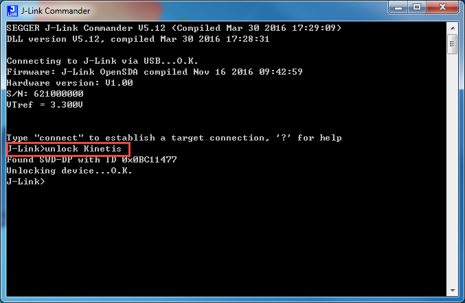
Customer could consider to use Segger J-Link commander tool to unlock the KM34Z256VLL7 product:
Have a great day,
Ma Hui
-----------------------------------------------------------------------------------------------------------------------
Note: If this post answers your question, please click the Correct Answer button. Thank you!
-----------------------------------------------------------------------------------------------------------------------
- 新着としてマーク
- ブックマーク
- 購読
- ミュート
- RSS フィードを購読する
- ハイライト
- 印刷
- 不適切なコンテンツを報告
Hello Hui Ma,
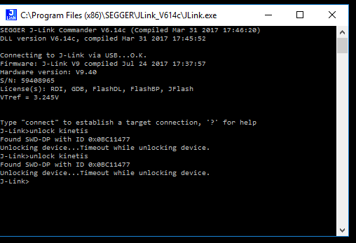
I tired that and got a timeout response. I've attached a screenshot for your reference.
Thanks,
Arvind
- 新着としてマーク
- ブックマーク
- 購読
- ミュート
- RSS フィードを購読する
- ハイライト
- 印刷
- 不適切なコンテンツを報告
Hi Arvind,
I would recommend to use below thread attached J-Link Command script file:
Thread link is below:
https://community.nxp.com/thread/439921
Wish it helps.
Have a great day,
Ma Hui
-----------------------------------------------------------------------------------------------------------------------
Note: If this post answers your question, please click the Correct Answer button. Thank you!
-----------------------------------------------------------------------------------------------------------------------
- 新着としてマーク
- ブックマーク
- 購読
- ミュート
- RSS フィードを購読する
- ハイライト
- 印刷
- 不適切なコンテンツを報告
Hello Hui Ma,
Nothing seems to be working. We had few more boards mounted but all go into secure mode on the very first attempt to program the device.
Is there a way where we can check to see if we are unintentionally setting the mass erase and readout lock bits before we actually start programming?
Additional Info: Here's a log of the Jlink console of a very first attempt to program a fresh device
------------------------------------------------
Application log started
- J-Flash V6.14c (J-Flash compiled Mar 31 2017 17:46:07)
- JLinkARM.dll V6.14c (DLL compiled Mar 31 2017 17:45:52)
Reading flash device list [C:\Program Files\SEGGER\JLink_V614c\ETC\JFlash\Flash.csv] ...
- List of flash devices read successfully (451 Devices)
Reading MCU device list ...
- List of MCU devices read successfully (6407 Devices)
Creating new project ...
- New project created successfully
Connecting ...
- Connecting via USB to J-Link device 0
- Target interface speed: 4000 kHz (Fixed)
- VTarget = 2.989V
- ERROR: DAP error while reading AIRCR / CPUID register
- ERROR: Failed to connect.
Could not establish a connection to target.
-------------------------------------------------
Regards,
Arvind
- 新着としてマーク
- ブックマーク
- 購読
- ミュート
- RSS フィードを購読する
- ハイライト
- 印刷
- 不適切なコンテンツを報告
Hi Arvind,
For I don't have a valid J-Flash license, I could not try the J-Flash tool with TWR-KM34Z75M board.
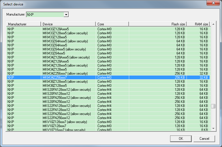
While, during the J-Flash project setup process, if you select below [MKM34Z256xxx7] device?
That will help to avoid program the secured value at flash address 0x40C (FTFA_FSEC).
Customer also could check the image file address 0x40C value, which will be loaded to FTFA_FSEC register during chip reset.
Have a great day,
Ma Hui
-----------------------------------------------------------------------------------------------------------------------
Note: If this post answers your question, please click the Correct Answer button. Thank you!
-----------------------------------------------------------------------------------------------------------------------


