- Forums
- Product Forums
- General Purpose MicrocontrollersGeneral Purpose Microcontrollers
- i.MX Forumsi.MX Forums
- QorIQ Processing PlatformsQorIQ Processing Platforms
- Identification and SecurityIdentification and Security
- Power ManagementPower Management
- Wireless ConnectivityWireless Connectivity
- RFID / NFCRFID / NFC
- Advanced AnalogAdvanced Analog
- MCX Microcontrollers
- S32G
- S32K
- S32V
- MPC5xxx
- Other NXP Products
- S12 / MagniV Microcontrollers
- Powertrain and Electrification Analog Drivers
- Sensors
- Vybrid Processors
- Digital Signal Controllers
- 8-bit Microcontrollers
- ColdFire/68K Microcontrollers and Processors
- PowerQUICC Processors
- OSBDM and TBDML
- S32M
- S32Z/E
-
- Solution Forums
- Software Forums
- MCUXpresso Software and ToolsMCUXpresso Software and Tools
- CodeWarriorCodeWarrior
- MQX Software SolutionsMQX Software Solutions
- Model-Based Design Toolbox (MBDT)Model-Based Design Toolbox (MBDT)
- FreeMASTER
- eIQ Machine Learning Software
- Embedded Software and Tools Clinic
- S32 SDK
- S32 Design Studio
- GUI Guider
- Zephyr Project
- Voice Technology
- Application Software Packs
- Secure Provisioning SDK (SPSDK)
- Processor Expert Software
- Generative AI & LLMs
-
- Topics
- Mobile Robotics - Drones and RoversMobile Robotics - Drones and Rovers
- NXP Training ContentNXP Training Content
- University ProgramsUniversity Programs
- Rapid IoT
- NXP Designs
- SafeAssure-Community
- OSS Security & Maintenance
- Using Our Community
-
- Cloud Lab Forums
-
- Knowledge Bases
- ARM Microcontrollers
- i.MX Processors
- Identification and Security
- Model-Based Design Toolbox (MBDT)
- QorIQ Processing Platforms
- S32 Automotive Processing Platform
- Wireless Connectivity
- CodeWarrior
- MCUXpresso Suite of Software and Tools
- MQX Software Solutions
- RFID / NFC
- Advanced Analog
-
- NXP Tech Blogs
- Home
- :
- General Purpose Microcontrollers
- :
- Kinetis Microcontrollers
- :
- Re: Completely Turning of Rx/Tx lines
Completely Turning of Rx/Tx lines
- Subscribe to RSS Feed
- Mark Topic as New
- Mark Topic as Read
- Float this Topic for Current User
- Bookmark
- Subscribe
- Mute
- Printer Friendly Page
Completely Turning of Rx/Tx lines
- Mark as New
- Bookmark
- Subscribe
- Mute
- Subscribe to RSS Feed
- Permalink
- Report Inappropriate Content
Greetings,
I am using KDS v3.2 with Processor expert on a MK22FN256LVH12 on a Custom board.
I am currently using a Bluetooth chip connected to the UART2 of chip, and I've noticed that even when I turn the bluetooth chip off, and turn the reset low (resetting it) that my UART lines remain at 3.3V. This is even when I set the microcontroller to VLSS1 to sleep.
I've tried setting the UART pins to pulldown, pullup, open drain, no open drain, basically anything to see if the pin settings will stop it from being awake. Any suggestions or thoughts would be appreciated!
- Mark as New
- Bookmark
- Subscribe
- Mute
- Subscribe to RSS Feed
- Permalink
- Report Inappropriate Content
Before enter low power mode, please try to configure the pin as GPIO function and then output low voltage.
When you want these pins act as UART function, then you need to reconfigure them as UART pins.(PORTx_PCRn[MUX])
Best Regards,
Robin
-----------------------------------------------------------------------------------------------------------------------
Note: If this post answers your question, please click the Correct Answer button. Thank you!
-----------------------------------------------------------------------------------------------------------------------
- Mark as New
- Bookmark
- Subscribe
- Mute
- Subscribe to RSS Feed
- Permalink
- Report Inappropriate Content
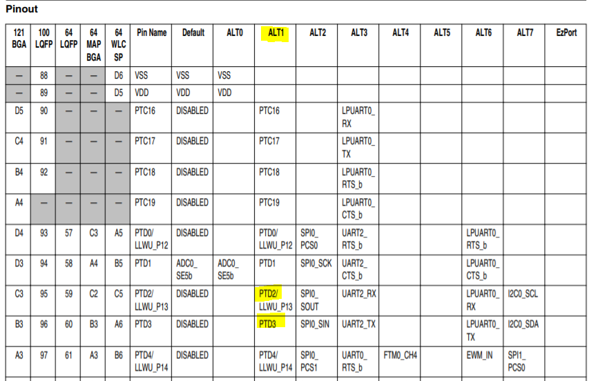
So the two pins I'm working on are pins 59 and 60 on the 64 pin MK22FN micro, thus my code I thought was correct is shown below, but that doesn't seem correct. What am I missing?
PORTD_PCR2 |= (PORT_PCR_MUX(1));
PORTD_PCR3 |= (PORT_PCR_MUX(1));
////
GPIOD_PDOR = GPIOD_PDOR & (0xFFFFFFFB);
GPIOD_PDOR = GPIOD_PDOR & (0xFFFFFFF7);
- Mark as New
- Bookmark
- Subscribe
- Mute
- Subscribe to RSS Feed
- Permalink
- Report Inappropriate Content
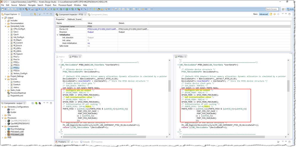
Considering that you are using Processor Expert, you can refer the function generated by Processor Expert.
/* Enable device clock gate */
/* SIM_SCGC5: PORTD=1 */
SIM_SCGC5 |= SIM_SCGC5_PORTD_MASK;
/* Configure pin as output */
/* GPIOD_PDDR: PDD|=4 */
GPIOD_PDDR |= GPIO_PDDR_PDD(0x04);
/* Set initialization value */
/* GPIOD_PDOR: PDO|=4 */
GPIOD_PDOR |= GPIO_PDOR_PDO(0x04);
/* Initialization of pin routing */
/* PORTD_PCR2: ISF=0,MUX=1 */
PORTD_PCR2 = (uint32_t)((PORTD_PCR2 & (uint32_t)~(uint32_t)(
PORT_PCR_ISF_MASK |
PORT_PCR_MUX(0x06)
)) | (uint32_t)(
PORT_PCR_MUX(0x01)
));
/* SIM_SCGC5: PORTD=1 */
SIM_SCGC5 |= SIM_SCGC5_PORTD_MASK;
/* Configure pin as output */
/* GPIOD_PDDR: PDD|=8 */
GPIOD_PDDR |= GPIO_PDDR_PDD(0x08);
/* Set initialization value */
/* GPIOD_PDOR: PDO|=8 */
GPIOD_PDOR |= GPIO_PDOR_PDO(0x08);
/* Initialization of pin routing */
/* PORTD_PCR3: ISF=0,MUX=1 */
PORTD_PCR3 = (uint32_t)((PORTD_PCR3 & (uint32_t)~(uint32_t)(
PORT_PCR_ISF_MASK |
PORT_PCR_MUX(0x06)
)) | (uint32_t)(
PORT_PCR_MUX(0x01)
));
Best Regards,
Robin
-----------------------------------------------------------------------------------------------------------------------
Note: If this post answers your question, please click the Correct Answer button. Thank you!
-----------------------------------------------------------------------------------------------------------------------
- Mark as New
- Bookmark
- Subscribe
- Mute
- Subscribe to RSS Feed
- Permalink
- Report Inappropriate Content
Thank you. This worked to the same extent that bobpaddock's example that I modified did. The TX line seems to stay low now, but the RX remains at 2.7V. The board now draws a lot more current when it is trying/in sleep mode. 1.3mA without the code change and 35mA with, even though the pins are set to be low. Any thoughts?
- Mark as New
- Bookmark
- Subscribe
- Mute
- Subscribe to RSS Feed
- Permalink
- Report Inappropriate Content
Assign not OR the MUX value.
ORing MUX(1) with the MUX(UART) value will give something you probably don't want.
Having 'Magic Numbers' like 0xFFFFFFFx in code is in general bad practice.
#define or enum a mask, or preferably use something from the manufactures header file to create the mask.
No one, including you years from now, will know what those values mean to help you if that is the issue.
- Mark as New
- Bookmark
- Subscribe
- Mute
- Subscribe to RSS Feed
- Permalink
- Report Inappropriate Content
I see that is a good point about magic numbers. So here is my revision, but I still do not see a change.
PORTD_PCR2 = 0001; //change mux to alt 1 which is GPIO
PORTD_PCR3 = 0001; //change mux to alt 1 which is GPIO
GPIOD_PDDR = 0x0C; //Pin is configured as general-purpose output
GPIOD_PDOR = 0x0; //Logic level 0 is driven on pin
- Mark as New
- Bookmark
- Subscribe
- Mute
- Subscribe to RSS Feed
- Permalink
- Report Inappropriate Content
PORTD_PCR2 = 0001; //change mux to alt 1 which is GPIO
PORTD_PCR3 = 0001; //change mux to alt 1 which is GPIO
GPIOD_PDDR = 0x0C; //Pin is configured as general-purpose outputGPIOD_PDOR = 0x0; //Logic level 0 is driven on pin
Went a little to far in reducing the code.
Still need the MUX() as it hides shifts and masks.
Still need the AND for the GIO. Only want to change one pin, not all of them.
Something along this line:
#define MEANINGFUL_NAME_bm (0x00000040UL)
/* _bm means Bit Mask */
PORTD_PCR2 = PORT_PCR_MUX(1U);
PORTD_PCR3 = PORT_PCR_MUX(1U);
GPIOD_PDOR &= ~MEANINGFUL_NAME_bm; /* Drive output low */
GPIOD_PDDR &= ~MEANINGFUL_NAME_bm; /* Set pin to output [Check data sheet to see if this should be a OR, don't have data sheet at hand] */
Note that I swapped PDOR and PDDR to prevent a short glitch on the output.
- Mark as New
- Bookmark
- Subscribe
- Mute
- Subscribe to RSS Feed
- Permalink
- Report Inappropriate Content
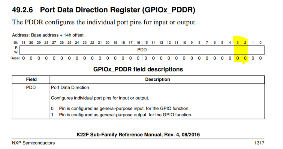
I believe it is an OR...With the bit mask why did you choose 0x040? If its pins 2 and 3 of port D wouldn't it be 0xC? Shown here?
Using your example it successfully turned one pin low, but the other hovers at 2.7 volts now and is draining a lot of current. Specifically Pin 59 which would be Port D pin 2.
This got one pin low... Which would be Port D pin 3 (pin 60)
#define MEANINGFUL_NAME_bm (0x00000040UL)
PORTD_PCR2 = PORT_PCR_MUX(1U);
PORTD_PCR3 = PORT_PCR_MUX(1U);
GPIOD_PDOR &= ~MEANINGFUL_NAME_bm; /* Drive output low */
GPIOD_PDDR |= ~MEANINGFUL_NAME_bm;
- Mark as New
- Bookmark
- Subscribe
- Mute
- Subscribe to RSS Feed
- Permalink
- Report Inappropriate Content
The 0x40 was an arbitrary number, I picked.
As I said didn't have data sheet at hand.
0x0C would be correct as you showed.
For an OR not not use the compliment operator '~'.
- Mark as New
- Bookmark
- Subscribe
- Mute
- Subscribe to RSS Feed
- Permalink
- Report Inappropriate Content
Should read 'OR do not use...'.


