- Forums
- Product Forums
- General Purpose MicrocontrollersGeneral Purpose Microcontrollers
- i.MX Forumsi.MX Forums
- QorIQ Processing PlatformsQorIQ Processing Platforms
- Identification and SecurityIdentification and Security
- Power ManagementPower Management
- Wireless ConnectivityWireless Connectivity
- RFID / NFCRFID / NFC
- Advanced AnalogAdvanced Analog
- MCX Microcontrollers
- S32G
- S32K
- S32V
- MPC5xxx
- Other NXP Products
- S12 / MagniV Microcontrollers
- Powertrain and Electrification Analog Drivers
- Sensors
- Vybrid Processors
- Digital Signal Controllers
- 8-bit Microcontrollers
- ColdFire/68K Microcontrollers and Processors
- PowerQUICC Processors
- OSBDM and TBDML
- S32M
- S32Z/E
-
- Solution Forums
- Software Forums
- MCUXpresso Software and ToolsMCUXpresso Software and Tools
- CodeWarriorCodeWarrior
- MQX Software SolutionsMQX Software Solutions
- Model-Based Design Toolbox (MBDT)Model-Based Design Toolbox (MBDT)
- FreeMASTER
- eIQ Machine Learning Software
- Embedded Software and Tools Clinic
- S32 SDK
- S32 Design Studio
- GUI Guider
- Zephyr Project
- Voice Technology
- Application Software Packs
- Secure Provisioning SDK (SPSDK)
- Processor Expert Software
- Generative AI & LLMs
-
- Topics
- Mobile Robotics - Drones and RoversMobile Robotics - Drones and Rovers
- NXP Training ContentNXP Training Content
- University ProgramsUniversity Programs
- Rapid IoT
- NXP Designs
- SafeAssure-Community
- OSS Security & Maintenance
- Using Our Community
-
- Cloud Lab Forums
-
- Knowledge Bases
- ARM Microcontrollers
- i.MX Processors
- Identification and Security
- Model-Based Design Toolbox (MBDT)
- QorIQ Processing Platforms
- S32 Automotive Processing Platform
- Wireless Connectivity
- CodeWarrior
- MCUXpresso Suite of Software and Tools
- MQX Software Solutions
- RFID / NFC
- Advanced Analog
-
- NXP Tech Blogs
- Home
- :
- General Purpose Microcontrollers
- :
- Kinetis Microcontrollers
- :
- Re: After the JTAG_TCLK/ SWD_CLK pin multiple as GPIO,and then cannot download the program anymore!
After the JTAG_TCLK/ SWD_CLK pin multiple as GPIO,and then cannot download the program anymore!
- Subscribe to RSS Feed
- Mark Topic as New
- Mark Topic as Read
- Float this Topic for Current User
- Bookmark
- Subscribe
- Mute
- Printer Friendly Page
After the JTAG_TCLK/ SWD_CLK pin multiple as GPIO,and then cannot download the program anymore!
- Mark as New
- Bookmark
- Subscribe
- Mute
- Subscribe to RSS Feed
- Permalink
- Report Inappropriate Content
After the JTAG_TCLK/ SWD_CLK pin multiple as GPIO,and then cannot download the program anymore!
Please help me,thanks!
- Mark as New
- Bookmark
- Subscribe
- Mute
- Subscribe to RSS Feed
- Permalink
- Report Inappropriate Content
Hi everyone,
Thanks for your attentions. Now my board can work again under a warm - hearted man's great answer, as the following websit.
Your kindly attention is enough to warm a world. Have a good day and wish you good luck.
qzy
- Mark as New
- Bookmark
- Subscribe
- Mute
- Subscribe to RSS Feed
- Permalink
- Report Inappropriate Content
Hello,
So you are using the NXP TWR-KE18F? If yes, then please make reference below post on how to re-flash the board.
- Mark as New
- Bookmark
- Subscribe
- Mute
- Subscribe to RSS Feed
- Permalink
- Report Inappropriate Content
Hi,
Yes,I am using the NXP TWR-KE18F512VLL16. I try it, but it also doesn't work.
Thanks, looking for your further attention, and have a good day.
qzy
- Mark as New
- Bookmark
- Subscribe
- Mute
- Subscribe to RSS Feed
- Permalink
- Report Inappropriate Content
Hi
See chapter 23 in the KE1xF user's manual and https://www.nxp.com/docs/en/user-guide/KFLLDRUG.pdf :
regards
Mark
- Mark as New
- Bookmark
- Subscribe
- Mute
- Subscribe to RSS Feed
- Permalink
- Report Inappropriate Content
Hi Mark,
I have seen it. Ridiculously,I am a little silly and don't know what to do.
Hopefully you can write a step so that I can do with it.
Thanks. Have a good day.
qzy
- Mark as New
- Bookmark
- Subscribe
- Mute
- Subscribe to RSS Feed
- Permalink
- Report Inappropriate Content
Hi
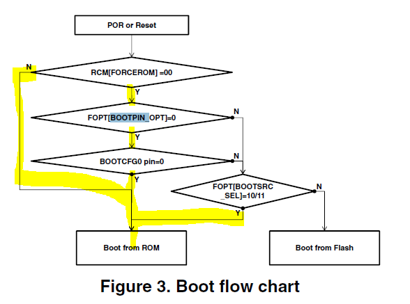
1. Connect BOOTCFG0 to GND
The BOOTCFG0 pin location is not specified in the KE18's documentation so you may need to ask NXP where it is located.
2. Connect a serial interface to LPUART0 (PTB1 and PTB2) or LPUART 1 (PTC6 and PTC7)
3. Run the KinetisFlashTool on the PC
4. Connect to the board
5. Command an erase
Regards
Mark
P.S. It is possible that the boot loader is disabled (in the flash configuration) in which case you may need to get a new board and be very careful to not do the same configuration.
- Mark as New
- Bookmark
- Subscribe
- Mute
- Subscribe to RSS Feed
- Permalink
- Report Inappropriate Content
Hi Mark,
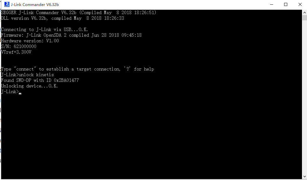
Here is not a phone number of NXP. So, today, I retry to input the "unlock kinetis" command with the J-LINK commander tool. It seems to be working and it writes that "Found SWD-DP with ID 0x2BA01477 Unlocking device...O.K."
But when I turn buck to bootloader mode, it is also cannot dowload program.
After the command--"unlock kinetis" works out , what should I do.
Looking for your help.Have a good day.
qzy
- Mark as New
- Bookmark
- Subscribe
- Mute
- Subscribe to RSS Feed
- Permalink
- Report Inappropriate Content
Hi
I don't think that the un-secure command is what you need (this won't necessarily change the loaded code from disabling the pins) - you need the mass erase command to restart with a "fresh" chip.
Regards
Mark
- Mark as New
- Bookmark
- Subscribe
- Mute
- Subscribe to RSS Feed
- Permalink
- Report Inappropriate Content
Hi, Mark
So,What is the mass erase command.
Looking for your reply.
qzy
- Mark as New
- Bookmark
- Subscribe
- Mute
- Subscribe to RSS Feed
- Permalink
- Report Inappropriate Content
Hi
Try holding the CPU in reset (eg. by holding reset button) when you connect to the board with the debugger.
While the debugger is trying to connect release the reset button and it may then have time to take control of the processor before the pins are reconfigured.
Alternatively try setting the debugger option to "erase on connection". This often also allows it to recover for such states.
Regards
Mark
uTasker developer and supporter (+5'000 hours experience on +60 Kinetis derivatives in +80 product developments)
Kinetis: http://www.utasker.com/kinetis.html
uTasker - for more performance and faster, cheaper product development
- Mark as New
- Bookmark
- Subscribe
- Mute
- Subscribe to RSS Feed
- Permalink
- Report Inappropriate Content
Hi Mark,
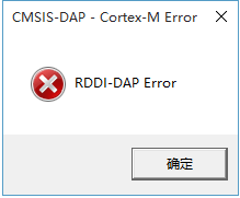
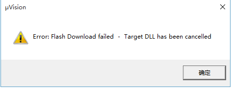
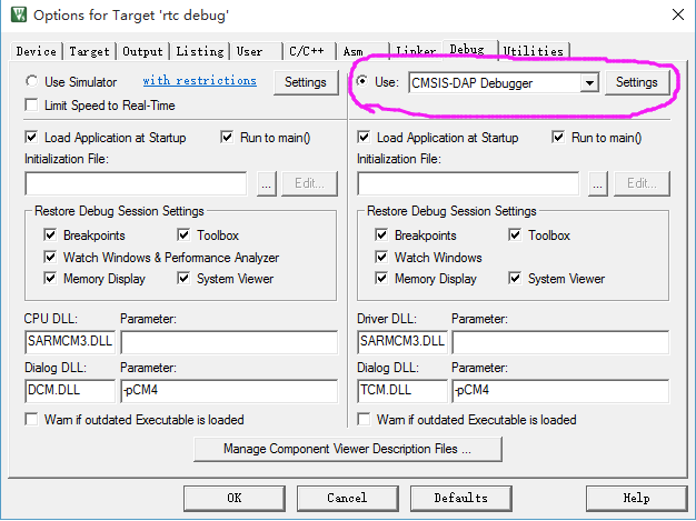
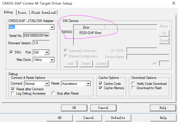
Thanks for your reply. I've tried it under your guidline, but it doesn't work. My board cannot identify the "CMSIS-DAP".
The situation is as follows.
Looking for your futher discussion.Have a good day.
qzy
- Mark as New
- Bookmark
- Subscribe
- Mute
- Subscribe to RSS Feed
- Permalink
- Report Inappropriate Content
Hi
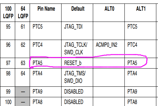
Have you also disabled/reconfigured the reset pin?
If you, this may make it difficult or even impossible for the debugger to be able to communicate.
What you can also do is to use the KE18's internal boot loader (Kboot) to erase the flash with and thus recover the device.
Regards
Mark
- Mark as New
- Bookmark
- Subscribe
- Mute
- Subscribe to RSS Feed
- Permalink
- Report Inappropriate Content
Hi Mark,
I may be reconfigure the reset pin as a GPIO. It cannot be recovered anymore?
Moreover, how to use the KE18's internal boot loader (Kboot) to erase the flash? Would you tell me more futher.
Thanks,have a good day.
qzy
- Mark as New
- Bookmark
- Subscribe
- Mute
- Subscribe to RSS Feed
- Permalink
- Report Inappropriate Content
Hello,
Please let me know what NXP part are you using?
- Mark as New
- Bookmark
- Subscribe
- Mute
- Subscribe to RSS Feed
- Permalink
- Report Inappropriate Content
Hello Fang Li,
Thanks for your reply.The NXP board what I using is MKE18F512VLL16.
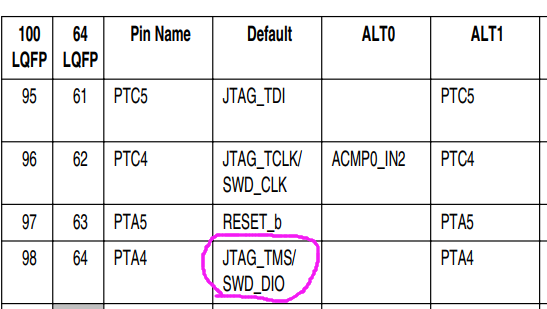
It shall be the JTAG/SWD pin being multiplexed as GPIO.And then,I cannot dowload program again
- Mark as New
- Bookmark
- Subscribe
- Mute
- Subscribe to RSS Feed
- Permalink
- Report Inappropriate Content
Hello Fang Li,
Thanks for your reply.The NXP board what I using is MKE18F512VLL16.
It shall be the JTAG/SWD pin being multiplexed as GPIO.And then,I cannot dowload program again.
