- Forums
- Product Forums
- General Purpose MicrocontrollersGeneral Purpose Microcontrollers
- i.MX Forumsi.MX Forums
- QorIQ Processing PlatformsQorIQ Processing Platforms
- Identification and SecurityIdentification and Security
- Power ManagementPower Management
- MCX Microcontrollers
- S32G
- S32K
- S32V
- MPC5xxx
- Other NXP Products
- Wireless Connectivity
- S12 / MagniV Microcontrollers
- Powertrain and Electrification Analog Drivers
- Sensors
- Vybrid Processors
- Digital Signal Controllers
- 8-bit Microcontrollers
- ColdFire/68K Microcontrollers and Processors
- PowerQUICC Processors
- OSBDM and TBDML
- S32M
-
- Solution Forums
- Software Forums
- MCUXpresso Software and ToolsMCUXpresso Software and Tools
- CodeWarriorCodeWarrior
- MQX Software SolutionsMQX Software Solutions
- Model-Based Design Toolbox (MBDT)Model-Based Design Toolbox (MBDT)
- FreeMASTER
- eIQ Machine Learning Software
- Embedded Software and Tools Clinic
- S32 SDK
- S32 Design Studio
- GUI Guider
- Zephyr Project
- Voice Technology
- Application Software Packs
- Secure Provisioning SDK (SPSDK)
- Processor Expert Software
- MCUXpresso Training Hub
-
- Topics
- Mobile Robotics - Drones and RoversMobile Robotics - Drones and Rovers
- NXP Training ContentNXP Training Content
- University ProgramsUniversity Programs
- Rapid IoT
- NXP Designs
- SafeAssure-Community
- OSS Security & Maintenance
- Using Our Community
-
- Cloud Lab Forums
-
- Knowledge Bases
- ARM Microcontrollers
- i.MX Processors
- Identification and Security
- Model-Based Design Toolbox (MBDT)
- QorIQ Processing Platforms
- S32 Automotive Processing Platform
- Wireless Connectivity
- CodeWarrior
- MCUXpresso Suite of Software and Tools
- MQX Software Solutions
-
- Home
- :
- 通用微控制器
- :
- Kinetis微控制器
- :
- Re: ADC calibration register behavior on Kinetis K22
ADC calibration register behavior on Kinetis K22
ADC calibration register behavior on Kinetis K22
Hi,
I'm facing on a problem, that is, it's difficult to satisfy the settling time required described in section 3.2.4 in this document, since the output impedance (RIN in the document) of a sensor device I'm using was pretty higher than I'd expected. I know it's our hardware design problem and the best way is to reduce the impedance using op-amp or something like that, but I'm still looking for a workaround to give a relief to products that we'd already have shipped.
While investigating this problem, I found an interesting symptom.
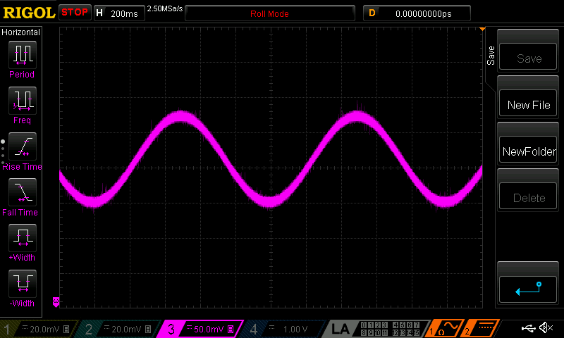
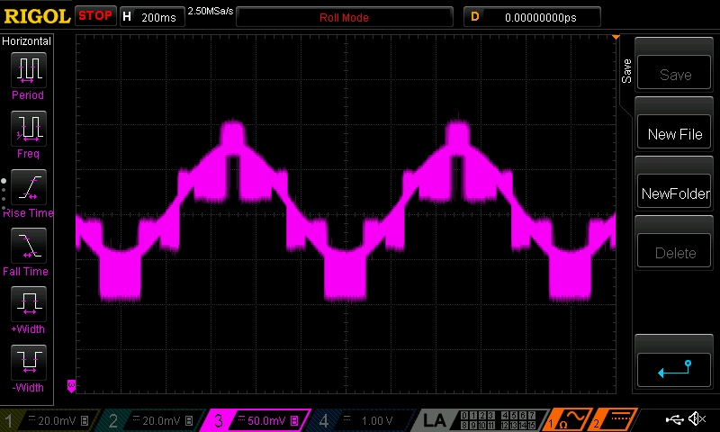
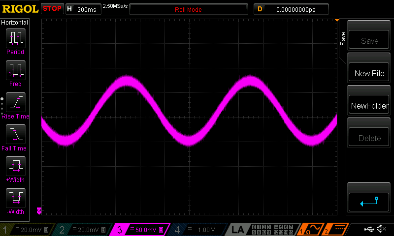
The left figure shows the input signal, and the right is also an input signal to K22 while ADC is running.
More interestingly,
The left figure shows the signal when all values on calibration registers were default value (ADCx_CLP0 = 32, ADCx_CLP1 = 64, ADCx_CLP2 = 128...). It clearly shows that the charging current to S/H capacitor depends on the values written to ADC calibration register, and finally, I found I could minimize charging current by writing zeros to all calibration register except ADCx_PG/MG remains 0x8000 (right figure).
Could you let me know how K22 utilizes values written to calibration registers?
Thanks in advance,
Seki, Tsutomu
Hi, Tsutomu,
You can set up ADC register so that ADC can match with high impedance input source.
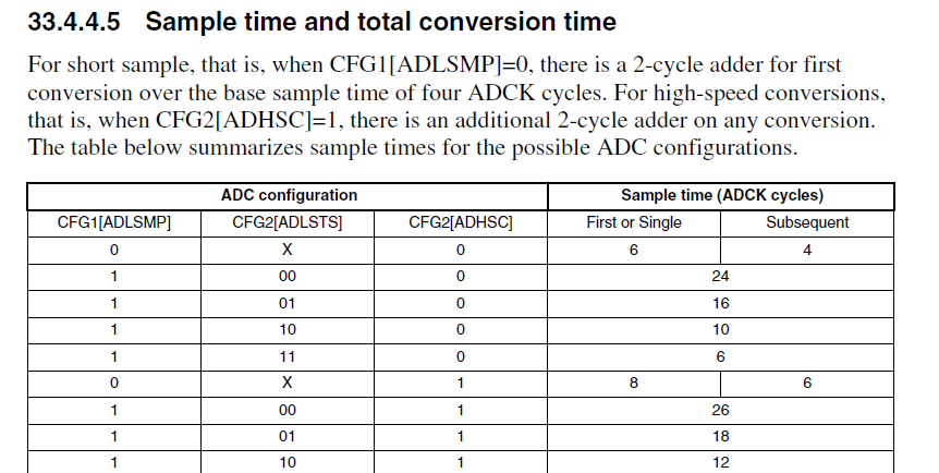
1)ADLSMP bit with ADCx_CFG1[ADLSMP]=1
2)CFG2[ADLSTS]=00;
3)CFG2[ADHSC]=1
The total sample time will be 26 AQDCK clock cycles.
Hope it can help you
BR
Xiangjun Rong
Hi, 湘君,
Thank you for your reply, but I know that... We have 32kΩ RIN and 0.01μF CIN on our production board. In this case, the time constant τ = 0.32ms and thus, to achieve sample time > 6.93 τ (for 10 bit conversion described in this document), we need ADCK less than 11.7kHz, but it's not possible since we don't have such a slow clock source.
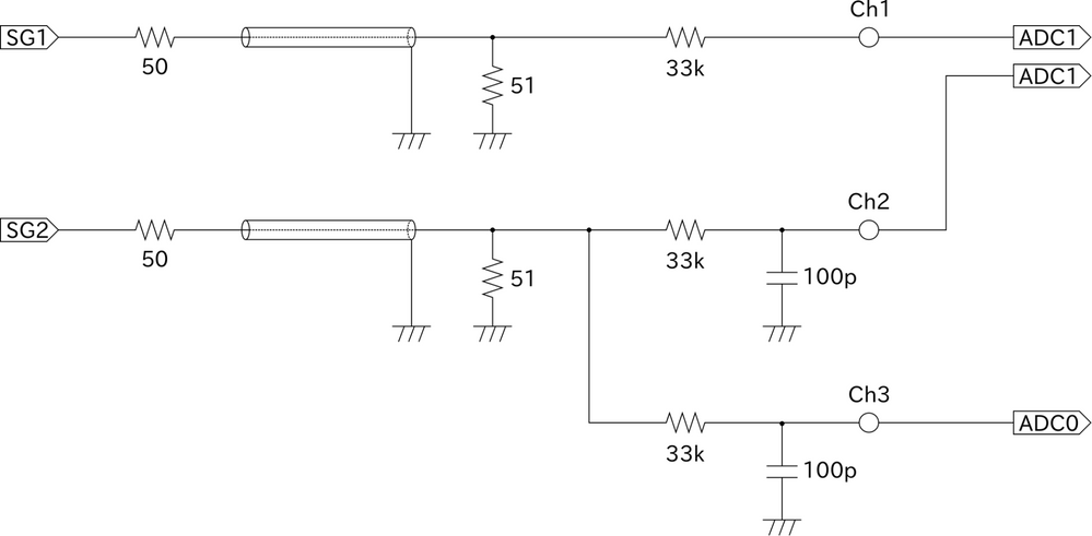
To visualize this problem, I've setup bread board as follows;
Here, ADC1 interleaves signal from signal generator ch1/2 (SG1/2) in the order ch1, ch1, ch2, ch2. The signal from SG2 is shared with ADC0/1. Please note that, R/C constants are different from out production board, because the purpose of this setup is not to reproduce the problem, but visualize the problem.
Then, I'd setup ADCs as follows;
| Register | ADC1 | ADC0 |
|---|---|---|
| ADCK | 1MHz | ← |
| ADLSTS | 10 ADCK | ← |
| ADTRG | H/W (PIT) @3200Hz | ← |
| MODE | single-ended 16-bit | ← |
| AVGS | 4 samples | ← |
| CLPx | defaults | all zeros |
| PG | 33280 (default value) | 32768 |
With this setup, I could capture this waveform.
I'd like to name first four set of glitches 1-1, 1-2, 1-3, 1-4 and second four sets 2-1, 2-2..., and so on.
Followings are details of them.
1-1~1-4 | 2-2~2-4 |
3-1~3-4 | 4-1~4-4 To be filled later... |
Cont'd to next post.
An another mysterious behavior comes with glitch 2-4.
After fourth SAR of second set has finished, DMA updates MUXSEL using this method. I suppose this has happened around 10.4μs.
Question 3: At this moment, it seems current flows from Ch1 to Ch2. Is this my optical illusion? I think it's not. Please clarify whether there is a moment that two gates (Ch1 and 2) are simultaneously opened or not.
I'd like to omit description about glitch 3-1 through 4-4, while it's almost same as glitch 1-1 through 2-4.
Then, let's see glitch happening on Ch2;
A rapid voltage drop on Ch2 should be "Inetrval.I" described in this document. According to the document. time constant for this voltage drop should be around 200ns, while Csh ≈ 8pF, Rsh ≈ 2kΩ, and CIN = 100pF. However, I can estimate time constant of this voltage drop is never more than 50ns. Note that "time constant" represents a time to charge to 63.2% of final voltage while we are talking about RC time constant.
Question 4: Please make it clear from where this time constant comes. Isn't there a route that detours Rsh? I guess there is a path that outputs "some voltage", as same reason as I asked in question 3.
Cont'd to next post.
It is clear that "some voltage" is related to values written into ADC calibration register "CLPx."
The left waveform shows the response when CLPx registers of ADC1 are all default values, and right shows when ADC1 was calibrated. They are completely different! Please note that here, CLPx registers of ADC0 are all zeros as I mentioned at first of first of the series of these posts. From these figures, I can say, we can minimize the distortion by writing all zeros to CLPx registers.
I want to write zeros to CLPx registers, while K22 ADC calibration does not behaves as expected (I think it's a glitch, otherwise please give us an evidence), however, ADC results non-monotonic and/or missing code in this case.
Then, my final questions are;
Question 5: Please let me know, how K22 utilizes values written to calibration registers. I'ts an important information for us to compensate converted values offline. I can calibrate ADC using histogram method, but it is estimated to take more than 24H to calibrate precisely. I want to generate INL table using ADC calibration result.
Question 6: Please let me know, what is done on each ADCK cycles. It's also important for us to know theoretical response of ADC results through hardware averages for more precised acquisition.
Question 7: Please let me know, what the "some voltage" is. Although I'm not sure, from observed waveform, I suppose it's related to 6 bits of MSBs of converted value.
Best Regards,
関 力 (Seki, Tsutomu)
Expanding glitch 1-1, you may able to see three discontinuities;
first discontinuity at -13μs, second at 0μs, third at 19μs.
I guess K22 has started sampling (gate ON) at -13μs, and hold (gate OFF) at 0μs, run SAR until 19μs, and gate ON again at 19μs for next sample.
Question 1: According to section 34.4.4.5 "Sample time and total conversion time" in this document, sampling time should be 10 ADCK cycles, regardless to first or subsequent sampling. What is this 3 extra sampling clocks?
From expansion of glitch 1-2 and 1-3, you may also able to see 2 extra sampling clocks;
1-2: second gate ON at -12μs | 1-2: third gate ON at -12μs |
The last one is glitch 1-4.
You may able to see fourth gate ON at -12μs, and fifth gate ON at 19μs, and gate OFF at 20μs.
Question 2: Is fifth gate ON expected? If yes, please make it clear why it's needed, otherwise, this symptom should be a hardware bug. As far as I understood, this gate ON is not required, while fourth SAR has already be done for AVGS = 4.
Cont'd to next post.
