- Forums
- Product Forums
- General Purpose MicrocontrollersGeneral Purpose Microcontrollers
- i.MX Forumsi.MX Forums
- QorIQ Processing PlatformsQorIQ Processing Platforms
- Identification and SecurityIdentification and Security
- Power ManagementPower Management
- Wireless ConnectivityWireless Connectivity
- RFID / NFCRFID / NFC
- Advanced AnalogAdvanced Analog
- MCX Microcontrollers
- S32G
- S32K
- S32V
- MPC5xxx
- Other NXP Products
- S12 / MagniV Microcontrollers
- Powertrain and Electrification Analog Drivers
- Sensors
- Vybrid Processors
- Digital Signal Controllers
- 8-bit Microcontrollers
- ColdFire/68K Microcontrollers and Processors
- PowerQUICC Processors
- OSBDM and TBDML
- S32M
- S32Z/E
-
- Solution Forums
- Software Forums
- MCUXpresso Software and ToolsMCUXpresso Software and Tools
- CodeWarriorCodeWarrior
- MQX Software SolutionsMQX Software Solutions
- Model-Based Design Toolbox (MBDT)Model-Based Design Toolbox (MBDT)
- FreeMASTER
- eIQ Machine Learning Software
- Embedded Software and Tools Clinic
- S32 SDK
- S32 Design Studio
- GUI Guider
- Zephyr Project
- Voice Technology
- Application Software Packs
- Secure Provisioning SDK (SPSDK)
- Processor Expert Software
- Generative AI & LLMs
-
- Topics
- Mobile Robotics - Drones and RoversMobile Robotics - Drones and Rovers
- NXP Training ContentNXP Training Content
- University ProgramsUniversity Programs
- Rapid IoT
- NXP Designs
- SafeAssure-Community
- OSS Security & Maintenance
- Using Our Community
-
- Cloud Lab Forums
-
- Knowledge Bases
- ARM Microcontrollers
- i.MX Processors
- Identification and Security
- Model-Based Design Toolbox (MBDT)
- QorIQ Processing Platforms
- S32 Automotive Processing Platform
- Wireless Connectivity
- CodeWarrior
- MCUXpresso Suite of Software and Tools
- MQX Software Solutions
- RFID / NFC
- Advanced Analog
-
- NXP Tech Blogs
- Home
- :
- CodeWarrior
- :
- QorIQ用CodeWarrior
- :
- Re: How copy data segment from FLASH to RAM using _rom_copy_info?
How copy data segment from FLASH to RAM using _rom_copy_info?
- RSS フィードを購読する
- トピックを新着としてマーク
- トピックを既読としてマーク
- このトピックを現在のユーザーにフロートします
- ブックマーク
- 購読
- ミュート
- 印刷用ページ
How copy data segment from FLASH to RAM using _rom_copy_info?
- 新着としてマーク
- ブックマーク
- 購読
- ミュート
- RSS フィードを購読する
- ハイライト
- 印刷
- 不適切なコンテンツを報告
When you have a flash based microcontroller the DEFAULT behaviour
is that the initialization code initializes the data section from a copy in flash.
To my surprise, this does not appear to be the case when compiling with Codewarrior.
- Why is this not documented?
I can see that the table for the __init_data is generated (_rom_copy_info).
It only contains entries where source and destination are the same
so nothing happens when this is called.
If I put ".data" in flash, then data variables are linked to flash.
If I put ".data" in internal RAM, then data variables are linked to RAM,
and the S-Record file will not put them in flash, it will put the data section in SRAM.
If I try to enable the "Generate ROM image", then I get all kinds of error/warnings about overlapping sections.
- Why do I get warnings, and how do I get rid of them?
- How do I set the ROM address?
There is no good explanation about the _rom_copy_info table.
I assume that the source and size comes from the segments.
- What mechanism sets the destination?
There are LOAD, BIND and ADDR commands to the linker.
The difference between these are not clear to me.
- Please explain the difference?
The documentation describes in detail how to prevent copying (using LOAD),
- Why not describe in detail how to copy?
I have a number of segments at 0x0000..0xCFF.
The .text segment starts at 0xD00.
- What do I set the ROM address to avoid getting overlap warnings?
I.E: "Overlap of the ROM image address of .bam section with executable address of .text section"
- 新着としてマーク
- ブックマーク
- 購読
- ミュート
- RSS フィードを購読する
- ハイライト
- 印刷
- 不適切なコンテンツを報告
Hi,
Let me answer your questinons below:
When you have a flash based microcontroller the DEFAULT behaviour
is that the initialization code initializes the data section from a copy in flash.
To my surprise, this does not appear to be the case when compiling with Codewarrior.
- Why is this not documented?
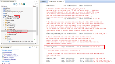
[NXP] This is actually the default configuration for the project created by the wizard - FLASH build configuration:
I can see that the table for the __init_data is generated (_rom_copy_info).
It only contains entries where source and destination are the same
so nothing happens when this is called.
If I put ".data" in flash, then data variables are linked to flash.
If I put ".data" in internal RAM, then data variables are linked to RAM,
and the S-Record file will not put them in flash, it will put the data section in SRAM.
[NXP] seems you are building RAM instead of FLASH build configuration.
If you select FLASH configuration Generated S-record contains only FLASH content.
If I try to enable the "Generate ROM image", then I get all kinds of error/warnings about overlapping sections.
- Why do I get warnings, and how do I get rid of them?
- How do I set the ROM address?
[NXP:] I assume you are basically adjusting RAM build configuration to be ROM/FLASH based. Such a change requires a different linker command file and therefore you may see many overlap warning.
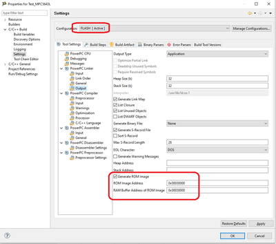
ROM Address should match with start address of your main flash block. Linker puts all the global data that needs to be initialized at the end of code block of this section. so in the example above the address is 0x30000 (see the linker file screenshot)
There is no good explanation about the _rom_copy_info table.
I assume that the source and size comes from the segments.
- What mechanism sets the destination?
[NXP] Actually the destination address comes from the memory segment definitions (for RAM sections e.g. .data it is RAM address). The source address (when Rom image is enabled) is generated by the linker and it is the address of flash copy of this section typically placed at the end of main flash block content. You can explicitly define the source address by LOAD linker command. In Ideal case you don't have to care about _rom_copy_info table. It is generated by the linker based on .lcf file.
There are LOAD, BIND and ADDR commands to the linker.
The difference between these are not clear to me.
- Please explain the difference?
[NXP]
LOAD: explicitly set where the rom image of a section should be placed into
ADDR: just returns the real start address of a section
BIND: defines absolute address placement of the section (kind of redundant functionality as AT command e.g." >internal_flash" at the end of section definiton). Not often used due to redundancy.
The documentation describes in detail how to prevent copying (using LOAD),
- Why not describe in detail how to copy?
Please check the compiler manual "" chapter 13 and 14". some examples are described there.
To prevent copying simply set the load address of the section using LOAD linker command to the same as destination address e.g. see the reset boot word example below:
MEMORY
{
  resetvector: org = 0x00000000, len = 0x00000010
 ...
}

SECTIONS
{
.__bam_bootarea LOAD (ADDR(resetvector)): {} > resetvector
...
source and destination addresses are equal = there is no copydown at startup. this section is placed into flash.
I have a number of segments at 0x0000..0xCFF.
The .text segment starts at 0xD00.
- What do I set the ROM address to avoid getting overlap warnings?
I.E: "Overlap of the ROM image address of .bam section with executable address of .text section"
[NXP] Take a look into memory blocks defined and set the one that .text is placed into as as ROM address. If it does not help please share your lcf file with us and we will suggest correct placement.
Some more Tips below:
ROM Image and RAM buffer addresses should be the same - it disables RAM buffering required by some obsolete PPC flash programmers. The address should point at the start address of your main flash section (this is usually the biggest flash block where code .text is placed into) and ROM sections are automatically placed at the end of used memory block of this section.
Every section from the linker command file generates it's ROM block if ROM generation is enabled.
The exception is the main flash block where start address matches with ROM image address.
So if there are multiple ROM/flash sections you shall "disable" creation of ROM sections for them by setting its ROM addresses to be same as the start address. e.g. interrupts_flash below:
MEMORY
{
    interrupts_flash:      org = 0x00040000,   len = 0x00001000
    internal_flash:        org = 0x00041000,   len = 0x00010000
    internal_ram:          org = 0x40006000,   len = 0x00001000
    stack_p1 :             org = 0x40007000,   len = 0x00000800 /* z0 Stack */
}

SECTIONS
{
    GROUP : {
      .ivor_branch_table_p1 (VLECODE) LOAD (ADDR(interrupts_flash))   : {}  //set LOAD address to 0x400000
      .intc_hw_branch_table_p1 LOAD (_e_ivor_branch_table_p1): {}   //set LOAD address to 0x400000 + size of previous section using linker generated symbol _e_ivor_branch_table_p1
      .__exception_handlers_p1 (VLECODE) LOAD (_e_intc_hw_branch_table_p1) : {}
    } > interrupts_flash

GROUP  : {
      .init : {}

      .init_vle (VLECODE) : {
        *(.init)
        *(.init_vle)
      }
      .text : {}

      .text_vle (VLECODE) : {
         *(.text)
         *(.text_vle)
       }

       .rodata (CONST) : {
         *(.rdata)
         *(.rodata)
       }
       .ctors : {}
       .dtors : {}
       extab : {}
       extabindex : {}
       Rom_addr_start = .;   //define a custom symbol - the start address where linker places the section images (not required)
    } > internal_flash

 GROUP : {
       .data   : {}   // ROM image of this section is stored at the next free address in internal_flash
       .bss   : {}
       .myRAM   : {}
...
If you would like to set the ROM address of particular section manually you can use LOAD()command which probably best fits with AT command.
.data LOAD(0x00001000): {} > internal_ram //ROM address = 0x1000; RAM address 0x40006000Instead of hardcoded address you can use commands e.g. ROMADDR or ADDR(). See the CodeWarrior build tools reference manual for more info about the commands.
The linker generates the initialization structures _rom_copy_info, _bss_init_info which are used by the default startup to perform ROM to RAM copydown + bss sections set to zero.
The linker also generates section start address/end address/ROM address for each section in .lcf (see the generated .map file):
e.g. for .data these symbols are available:
_f_data 40006000
_f_data_rom 00041770
_e_data 40006010
You can use these structures/symbols or create your own address symbols in .lcf.
For more information I'd recommend you to see the Build tools reference manual ("<CW MCU v11.0>\MCU\Help\PDF\MCU_Power-Architecture_Compiler.pdf "), section "Building a ROM Image".
Hope it helps.
Stan
- 新着としてマーク
- ブックマーク
- 購読
- ミュート
- RSS フィードを購読する
- ハイライト
- 印刷
- 不適切なコンテンツを報告
Sorry, but my changes are based on the FLASH configuration, not the RAM configuration.
I have now gotten it to work, but the functionality is non-intuitive and error prone.
I think you should update the documentation and explain in detail how
the ROM image functionality works, or better
- replace it with something easily understandable.
I see nowhere in the documentation how to select the "ROM image address" and "RAM address".
The documentation refers to flash programmers. That is irrelevant for most people.
I see nowhere in the documentation that when you select the "ROM image address" you
have to manually force all the other sections to an address.
The LOAD statements appears to be redundant, it is not clear that they are not.
============================
The only thing that should be needed is to tag the initialized data sections
I.E: something like:
GROUP {
.data :{} < internal_flash
} > internal_ram
or using your syntax:
.data LOAD(0x3800) :{} > internal_ram
This has enough information to place the data and to create the _rom_copy_info.
If you specify that the data section should be in internal ram and loaded from 0x00003800
in this way, then the S-Record file will end like this:
S315000031780100000000080000000400000100000033
S31500003188000C000000040000422D50535832302D28
S3150000319853504335363433324D4C5131000000001C
S31540000C004000143800000000000000000000000012
S31540000C100000471100000000000000000000000036
S31540000C20000000000000000000000000000000007E
S30940000C30FF0000007B
S7050000069460
The .data section is present in the S-Record file, but it is not located at 0x3800.
It is located at "0x40000C00" which is where my "internal_ram" starts.
Obviously, it is not going to work to flash such a file.
I consider this to be a bug.
As a comparison, the IAR C compiler handles ".data" in the following way:
initialize by copy { readwrite };
place in RAM_region { readwrite};
This is much less complex than your implementation.
Still, I have gotten it to work now but this has taken me a lot of time.
You should seriously think about your implementation.
- 新着としてマーク
- ブックマーク
- 購読
- ミュート
- RSS フィードを購読する
- ハイライト
- 印刷
- 不適切なコンテンツを報告
What processor are you using?
Which version CodeWarrior are you using?
- 新着としてマーク
- ブックマーク
- 購読
- ミュート
- RSS フィードを購読する
- ハイライト
- 印刷
- 不適切なコンテンツを報告
We are using the MPX5643L.
CodeWarrior 11.1 Special Edition.
I am currently working on a bootloader which will fit into 128 kB.
The rest of the team is using an older GCC, but since we are running out of code space,
the VLE functionality of the CodeWarrior is interesting.
- 新着としてマーク
- ブックマーク
- 購読
- ミュート
- RSS フィードを購読する
- ハイライト
- 印刷
- 不適切なコンテンツを報告
Hi,
FYI: Another option to consider is GCC toolchain with VLE support - S32 Design Studio for Power.
This might be easier migration path if the team is using older GCC.
See the release details here:
There is also separate community space for S32 Design Studio:
https://community.nxp.com/t5/S32-Design-Studio/bd-p/s32ds
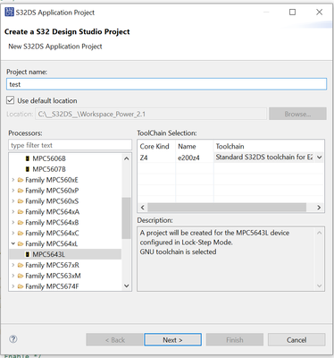
MPC5643L (lockstep mode) is supported by project wizard/debugger :
Hope it helps.
Stan


