
- Forums
- Product Forums
- General Purpose MicrocontrollersGeneral Purpose Microcontrollers
- i.MX Forumsi.MX Forums
- QorIQ Processing PlatformsQorIQ Processing Platforms
- Identification and SecurityIdentification and Security
- Power ManagementPower Management
- Wireless ConnectivityWireless Connectivity
- RFID / NFCRFID / NFC
- Advanced AnalogAdvanced Analog
- Neural Processing UnitsNeural Processing Units
- MCX Microcontrollers
- S32G
- S32K
- S32V
- MPC5xxx
- Other NXP Products
- S12 / MagniV Microcontrollers
- Powertrain and Electrification Analog Drivers
- Sensors
- Vybrid Processors
- Digital Signal Controllers
- 8-bit Microcontrollers
- ColdFire/68K Microcontrollers and Processors
- PowerQUICC Processors
- OSBDM and TBDML
- S32M
- S32Z/E
-
- Solution Forums
- Software Forums
- MCUXpresso Software and ToolsMCUXpresso Software and Tools
- CodeWarriorCodeWarrior
- MQX Software SolutionsMQX Software Solutions
- Model-Based Design Toolbox (MBDT)Model-Based Design Toolbox (MBDT)
- FreeMASTER
- eIQ Machine Learning Software
- Embedded Software and Tools Clinic
- S32 SDK
- S32 Design Studio
- GUI Guider
- Zephyr Project
- Voice Technology
- Application Software Packs
- Secure Provisioning SDK (SPSDK)
- Processor Expert Software
- Generative AI & LLMs
-
- Topics
- Mobile Robotics - Drones and RoversMobile Robotics - Drones and Rovers
- NXP Training ContentNXP Training Content
- University ProgramsUniversity Programs
- Rapid IoT
- NXP Designs
- SafeAssure-Community
- OSS Security & Maintenance
- Using Our Community
-
- Cloud Lab Forums
-
- Knowledge Bases
- ARM Microcontrollers
- i.MX Processors
- Identification and Security
- Model-Based Design Toolbox (MBDT)
- QorIQ Processing Platforms
- S32 Automotive Processing Platform
- Wireless Connectivity
- CodeWarrior
- MCUXpresso Suite of Software and Tools
- MQX Software Solutions
- RFID / NFC
- Advanced Analog
- Neural Processing Units
-
- NXP Tech Blogs
- Home
- :
- CodeWarrior
- :
- QorIQ用CodeWarrior
- :
- Re: DDR Validation Tool Tests Description
DDR Validation Tool Tests Description
- RSS フィードを購読する
- トピックを新着としてマーク
- トピックを既読としてマーク
- このトピックを現在のユーザーにフロートします
- ブックマーク
- 購読
- ミュート
- 印刷用ページ
DDR Validation Tool Tests Description

- 新着としてマーク
- ブックマーク
- 購読
- ミュート
- RSS フィードを購読する
- ハイライト
- 印刷
- 不適切なコンテンツを報告
Hello!
I am running a DDR validation test for my custom board based on T1042.
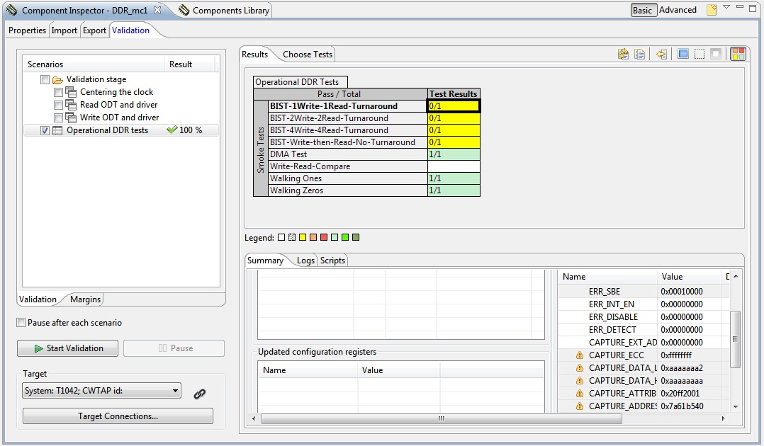
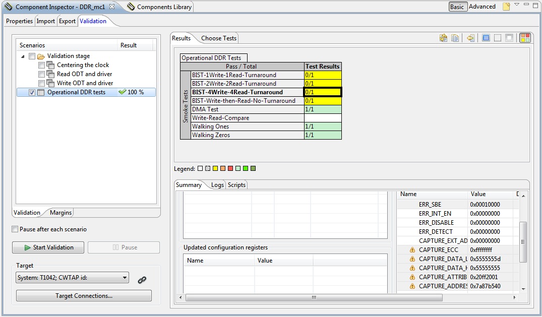
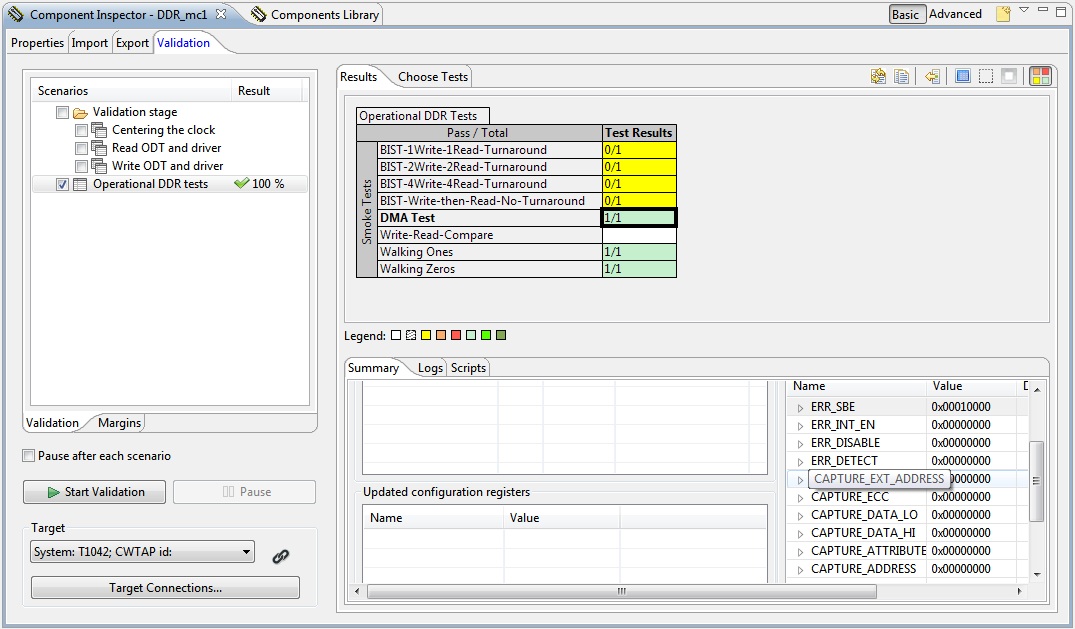
I want to understand the process of validation that what is actually happening when I run 1write-1read turnaround, 2write-2read turnaround, 4write-4read turnaround, Write then read no turnaround, DMA test, Walking ones and walking zeros tests.
Some of these are passing for my settings and some are failing for one configuration and the same results may fail for the next time and the test that is failing may get pass for the next test in my case.
So I want to know the working of these tests so that I can review my settings accordingly.
Regards,
Ather



 yipingwang
- 新着としてマーク
- ブックマーク
- 購読
- ミュート
- RSS フィードを購読する
- ハイライト
- 印刷
- 不適切なコンテンツを報告
Here are the details of DDR validation operational tests.
- 1write-1read turnaround
Runs the hardware built-in memory test. Occurs in several places throughout all of memory area defined by the chip select configuration [CSn_CONFIG and CSn_BNDS registers]. Total write/read streams will be 1 transaction each. The memory controller will check the data during this test. The test fails if memory mismatches are detected. The capture registers will hold information for the transaction that caused the first data miscompare. Note that transactions with ECC errors will take priority in the capture registers.
- 2write-2read turnaround
Runs the hardware built-in memory test. Occurs in several places throughout all of memory area defined by the chip select configuration [CSn_CONFIG and CSn_BNDS registers]. Total write/read streams will be 2 transactions each. The memory controller will check the data during this test. The test fails if memory mismatches are detected. The capture registers will hold information for the transaction that caused the first data miscompare. Note that transactions with ECC errors will take priority in the capture registers.
- 4write-4read turnaround
Runs the hardware built-in memory test. Occurs in several places throughout all of memory area defined by the chip select configuration [CSn_CONFIG and CSn_BNDS registers]. Total write/read streams will be 4 transactions each. The memory controller will check the data during this test. The test fails if memory mismatches are detected. The capture registers will hold information for the transaction that caused the first data miscompare. Note that transactions with ECC errors will take priority in the capture registers.
- Write then read no turnaround
Runs the hardware built-in memory test. Occurs in several places throughout all of memory area defined by the chip select configuration [CSn_CONFIG and CSn_BNDS registers]. Entire memory will be written before read transactions are issued. The memory controller will check the data during this test. The test fails if memory mismatches are detected. The capture registers will hold information for the transaction that caused the first data miscompare. Note that transactions with ECC errors will take priority in the capture registers.
- DMA test
DMA is configured using linked descriptors to transfer data from a source address to a destination address in DDR. The size of the data transferred is configurable. The source region is filled with a repeating pattern. After DMA finished the transfer, the test is reading back the data from the destination and compares it with the source data. The test fails at the first mismatch found.
- Walking ones
Writes a bit pattern that gradually sets [to 1] bits from LSB to MSB. Each byte is written multiple times depending on the selected access size, until each of the contained bits gets set, while the other ones are cleared. For each bit pattern, a write/read/compare sequence is performed. The test is repeated for each of the access size selected using the corresponding access size.
- walking zeros tests
Writes a bit pattern that gradually clears [sets to 0] bits from LSB to MSB. Each byte is written multiple times depending on the selected access size, until each of the contained bits gets cleared, while the other ones are set. For each bit pattern, a write/read/compare sequence is performed. The test is repeated for each of the access size selected using the corresponding access size.
- 新着としてマーク
- ブックマーク
- 購読
- ミュート
- RSS フィードを購読する
- ハイライト
- 印刷
- 不適切なコンテンツを報告
Thanks Yiping,
Can you please identify any problem in my board by looking at the error capture registers value. One more problem is that Sometimes my BIST 1write-1read test gets passed on the same settings and when I run thye test again, it gets failed. What might the possible issue ?
yipingwang
- 新着としてマーク
- ブックマーク
- 購読
- ミュート
- RSS フィードを購読する
- ハイライト
- 印刷
- 不適切なコンテンツを報告
Please refer to section "3 DDR4 design checklist" in the application note "AN5097, Hardware and Layout Design Considerations for DDR4 SDRAM Memory Interfaces - Application Not..." downloaded from "https://www.nxp.com/products/processors-and-microcontrollers/power-architecture/qoriq-communication-...".
