- Forums
- Product Forums
- General Purpose MicrocontrollersGeneral Purpose Microcontrollers
- i.MX Forumsi.MX Forums
- QorIQ Processing PlatformsQorIQ Processing Platforms
- Identification and SecurityIdentification and Security
- Power ManagementPower Management
- Wireless ConnectivityWireless Connectivity
- RFID / NFCRFID / NFC
- Advanced AnalogAdvanced Analog
- MCX Microcontrollers
- S32G
- S32K
- S32V
- MPC5xxx
- Other NXP Products
- S12 / MagniV Microcontrollers
- Powertrain and Electrification Analog Drivers
- Sensors
- Vybrid Processors
- Digital Signal Controllers
- 8-bit Microcontrollers
- ColdFire/68K Microcontrollers and Processors
- PowerQUICC Processors
- OSBDM and TBDML
- S32M
- S32Z/E
-
- Solution Forums
- Software Forums
- MCUXpresso Software and ToolsMCUXpresso Software and Tools
- CodeWarriorCodeWarrior
- MQX Software SolutionsMQX Software Solutions
- Model-Based Design Toolbox (MBDT)Model-Based Design Toolbox (MBDT)
- FreeMASTER
- eIQ Machine Learning Software
- Embedded Software and Tools Clinic
- S32 SDK
- S32 Design Studio
- GUI Guider
- Zephyr Project
- Voice Technology
- Application Software Packs
- Secure Provisioning SDK (SPSDK)
- Processor Expert Software
- Generative AI & LLMs
-
- Topics
- Mobile Robotics - Drones and RoversMobile Robotics - Drones and Rovers
- NXP Training ContentNXP Training Content
- University ProgramsUniversity Programs
- Rapid IoT
- NXP Designs
- SafeAssure-Community
- OSS Security & Maintenance
- Using Our Community
-
- Cloud Lab Forums
-
- Knowledge Bases
- ARM Microcontrollers
- i.MX Processors
- Identification and Security
- Model-Based Design Toolbox (MBDT)
- QorIQ Processing Platforms
- S32 Automotive Processing Platform
- Wireless Connectivity
- CodeWarrior
- MCUXpresso Suite of Software and Tools
- MQX Software Solutions
- RFID / NFC
- Advanced Analog
-
- NXP Tech Blogs
- Home
- :
- Topics
- :
- NXP Designs Knowledge Base
- :
- NFC DIN rail demo - how to do parametrization with NFC
NFC DIN rail demo - how to do parametrization with NFC
- Subscribe to RSS Feed
- Mark as New
- Mark as Read
- Bookmark
- Subscribe
- Printer Friendly Page
- Report Inappropriate Content
NFC DIN rail demo - how to do parametrization with NFC
NFC DIN rail demo - how to do parametrization with NFC
This post entry provides a detailed description of how an NFC DIN rail demo was developed so that you can leverage this knowledge to integrate NFC into your own system. This document has been structured as follows:
- Introduction
- NFC DIN rail demo functionality
- Wireless parametrization and zero power operation
- Wireless product diagnosis - Read light bulbs switching counters
- Wireless product diagnosis - Reset light bulbs switching counters
- Wireless firmware update
- NFC DIN rail hardware details
- Transformer PCB
- Switching PCB
- Explorer board and flex antenna
- Application logic and how NTAG I2C plus solution is used
- NTAG I2C plus product features
- How the NTAG I2C plus is used for wireless parametrization and zero power operation
- How the NTAG I2C plus is used for product diagnosis
- How the NTAG I2C plus is used for wireless firmware update
- MCU / Embedded software integration
- NTAG_I2C_Explorer_bootloader application workflow
- NTAG_I2C_Explorer_demo application workflow
- Phone / NFC device software integration
- NFC DIN rail Android demo application workflow
- Video recorded session
- Available resources
Introduction
The NFC DIN rail demo shows how NFC can be used for handling complex device settings on a mobile touchscreen. It is based on the NTAG I2C plus solution and demonstrates how NFC is used for:
- Wireless parametrization and zero power configuration.
- Wireless product diagnosis and troubleshooting.
- Wireless firmware update.
NFC DIN rail demo functionality
Industrial equipment such as circuit breakers, time relays, power units, sensors, etc typically come with limited user interfaces but with advanced settings and configurations. As NFC use becomes universal in smartphones and other handheld devices, these devices can be used as an external touchscreen interface enabling sophisticated interactions and configurability at a little cost.
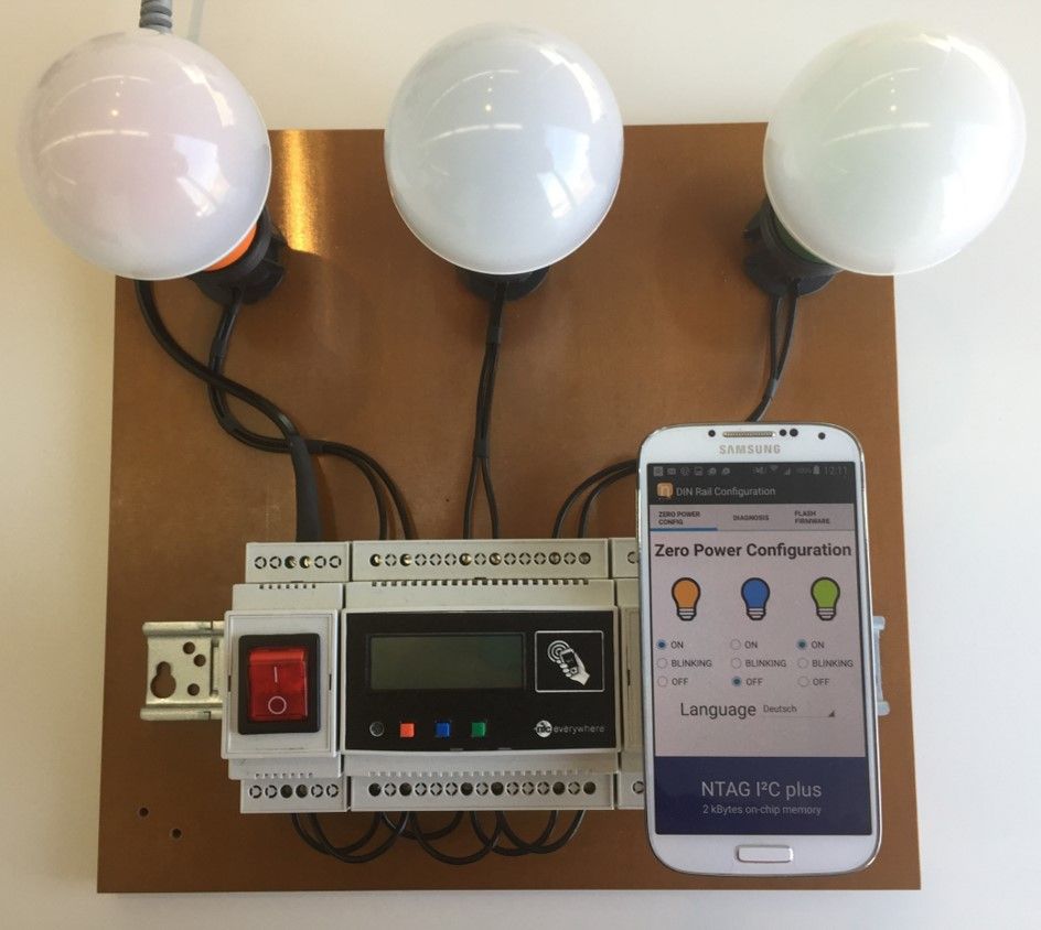
The NFC DIN rail demo could represent industrial equipment in charge of controling a lighting system. As a simplification, here it controls only three light bulbs. This DIN module consists of a power switch (220 V), an NFC interface and an LCD screen. Additionally, a dedicated phone application has been developed to interact with the NFC DIN rail for enabling wireless parametrization, wireless diagnosis and wireless firmware update via NFC.
Wireless parametrization and zero power operation
NFC can be used to save configuration settings so that equipment may be customized at any moment during its lifetime. Additionally, the energy harvesting feature, intrinsic to NFC, allow us to save product settings even if the device is unpowered (also called zero-power operation).
In this NFC DIN rail demo, the Android app let us set the light bulb status to ON, OFF or BLINKING and set the LCD language as well. After selecting the different settings on the screen, we tap the phones and the settings are saved into the module. The following video shows how this functionality works, also with the unit powered and unpowered.
Wireless product diagnosis - Read light bulbs switching counters
NFC can be used to get instant readouts of device status, usage, statistics and diagnosis data without dismounting the casing and even after a breakdown situation.
In this NFC DIN rail demo, the Android app lets us retrieve the switching counter values (the number of times the light bulbs have been switched ON / OFF). The following video shows how reading NFC DIN rail product diagnosis only takes one tap.
Wireless product diagnosis - Reset light bulbs switching counters
Additionally, the Android app lets us reset the switching counter values with a phone tap.
Wireless firmware update
With NFC, firmware upgrades can be done wirelessly, without cables, disks or other means of data transfer. It therefore, saves time since it is not necessary to dismount the device.
In this NFC DIN rail demo, the Android app lets us select the binary file to be flashed. This implementation is robust since you can retry as many times as needed, even if a failure occurs in the flashing operation. The following video shows how the NFC DIN rail firmware is updated to a firmware version introducing a faster light bulb blinking speed.
NFC DIN rail hardware details
Dismounting the DIN module is quite straightforward, especially if you are familiar with DIN casing.
- We unscrew and release the power wires coming from the power supply unit
- We unscrew and release the light bulb power wires
- We dismount the module from the rail and release it from the rail
- We open the boxing and see what is inside
The NFC DIN rail module consists of three PCBs: the Transformer PCB, the switching PCB and the Explorer board with a flex antenna
Transformer PCB
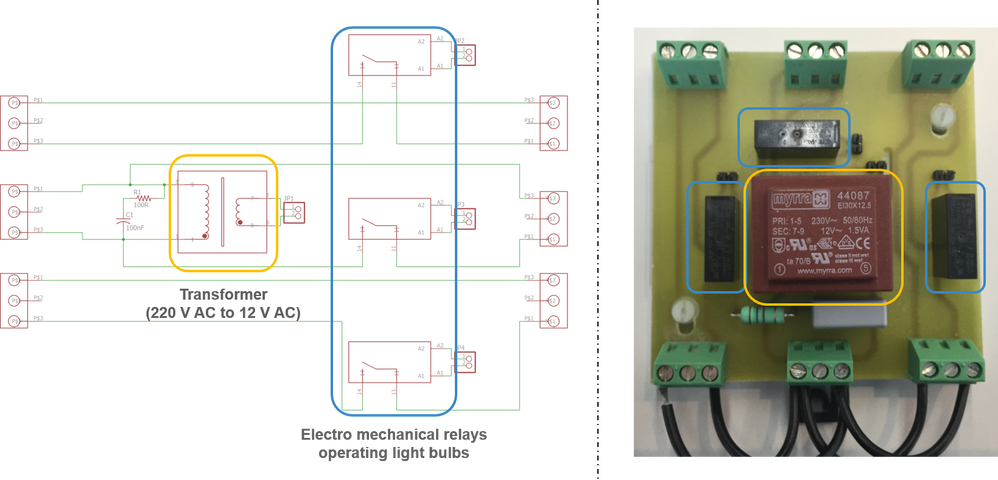
The transformer PCB includes three electromechanical relays that directly control the light bulbs. It also includes a transformer which converts the 220V AC supply from a standard socket to 12V AC. This 12V AC supply is used to power the switching PCB.
Switching PCB
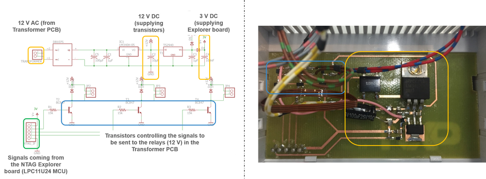
The switching PCB converts the 12V AC to 12V and 3V DC voltage supply. The 12V DC voltage is used to control the electromechanical relays, which in turn switches the light bulbs ON/ OFF. On the other hand, the 3V DC output is used to supply the Explorer board.
Explorer board and flex antenna
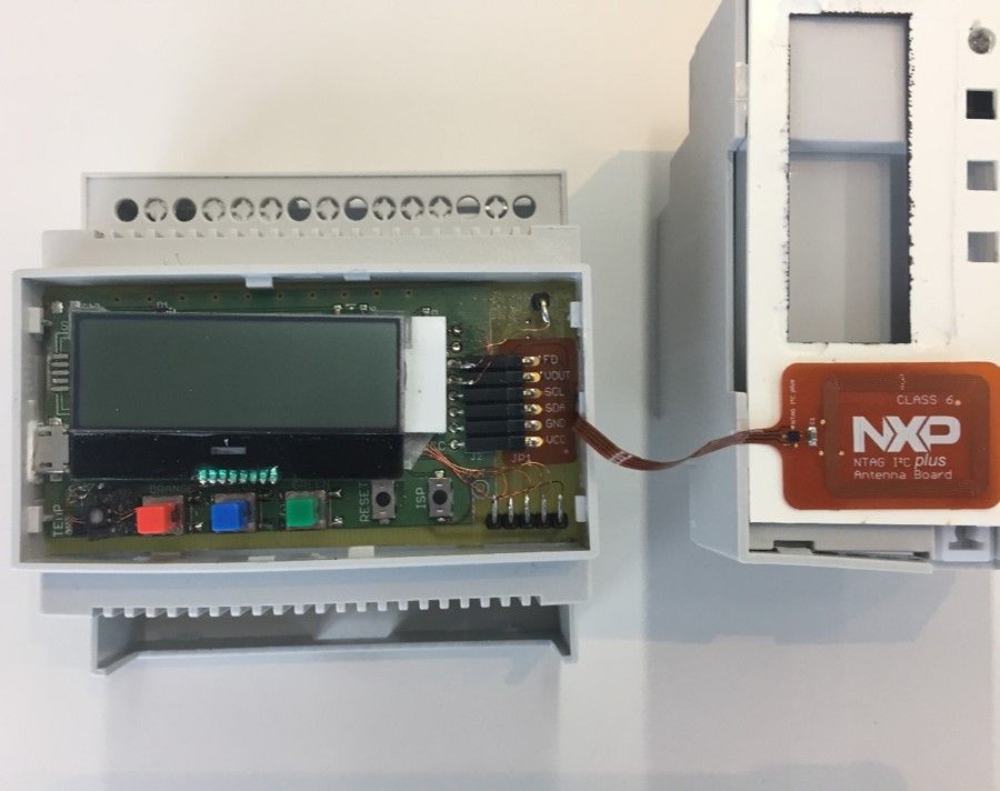
The Explorer board and flex antenna are part of the NTAG I2C plus support package. The Explorer board comes with: 5 push buttons, a temperature sensor, an LPC11U24 MCU, JTAG interface, LCD and I2C connectors. The NTAG I2C plus comes embedded in the Class 6 Flex antenna
All the design files for the Explorer board as well as the Flex antennas can be found in NT3H2111/2211|NXP
Application logic and how NTAG I2C plus solution is used
Before going into the implementation details, we briefly describe the NTAG I2C plus product.
NTAG I2C plus product features
The NTAG I2C plus is a family of connected NFC tags that combine a memory, a passive NFC interface with a contact I2C interface. As such, it supports full bidirectional communication between an NFC-enabled device and the host system's microcontroller, making it an ideal solution for NFC implementations that interface with a wide range of electronic devices. Additional to this dual interface solution, it has more features:
- A field detection pin to trigger external / connected devices.
- The energy harvesting, to power low consuming devices from the RF field.
- The SRAM buffer, a volatile memory without writing cycles limitations.
- The SRAM mirroring, for dynamic content update.
- The pass through mode, for fast data exchange between interfaces.
- Several memory access management settings from both NFC and I2C interfaces.
- And an originality check to detect clones.
More product details about NTAG I2C plus can be found at NT3H2111/2211|NXP and technical recorded videos are available in our training academy NFC Webinars|NXP.
How the NTAG I2C plus is used for wireless parametrization and zero power operation
The NTAG I2C plus EEPROM memory is used to store DIN module settings. The phone application is able to overwrite these bytes with the desired configuration. On power up, the MCU reads the saved settings and applies the corresponding configuration.
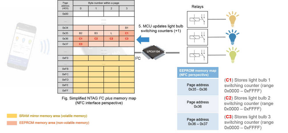
In this demo, one byte is used to configure each light bulb status ('0' - light bulb ON, '1' - light bulb OFF, '2' - light bulb BLINKS) and one byte used for the language configuration ( '0'- Deutsch, '1' -Babarian, '2' - Swiss, '3'- English, '4' - French). Using the Zero Power Config Android app tab, we define the desired settings. With a tap, the phone writes 4 bytes into the EEPROM memory (page addresses 0x34 - 0x35)
On power up, the NFC DIN module reads the EEPROM memory and:
- Changes the GPIO 17, 18 and 19 output configuration to HIGH or LOW accordingly
- Changes the language message on the LCD display.
Finally, the MCU updates the light bulbs switching counters by writing the EEPROM memory. Two bytes are used for the counters (page addresses 0x35-0x37)-
How the NTAG I2C plus is used for product diagnosis
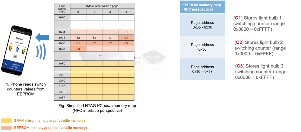
The product diagnosis provides two functionalities: read switching counters values and reset switching counters values. With a tap, the phone reads the EEPROM to retrieve the latest switching counter values.
Clicking on the Reset button and with a phone tap, we are actually overwriting the EEPROM by setting the switching counter values to '0'.
How the NTAG I2C plus is used for wireless firmware update
The NFC wireless firmware update capability in this demo leverages on two main aspects:
- First, the LPCs MCU capability to re-program the flash in the field without being removed from the PCB.
- Second, the NTAG I2C plus tag as a bridge to transfer data between the phone and the DIN module MCU.
The MCU flash memory can be re-programed using these two methods:
- In-System programming (ISP), which can program the on-chip flash memory using the system primary boot loader and programming interface. For instance, in the Explorer board, this can be done by connecting it via USB to a laptop (could also be UART, serial interface, etc).
- In-Application (IAP) programming, means that the application itself, the end-user code, can re-program the on-chip Flash memory
The LPC11U24 flash memory is grouped in 8 sectors of 4 kB each. The flash memory should be reprogrammed at the sector level. Another critical requirement is that the implementation must allow multiple FW updates and protection against failed FW update processes. For this, the firmware consists of two applications residing in flash:
- The first: the secondary bootloader application. This application is a piece of code starting at memory Sector 0. It implements the IAP functions allowing a certain flash memory area to be flashed and the logic to handle the NFC data transmission. This source code occupies 4 sectors.
- The second: is the user application code. It starts at the next free memory sector (in this case, it resides in sector 4 onwards), and is the flash memory area, which is overwritten when the NFC wireless firmware update is performed.
In this approach, the secondary bootloader application is not overwritten. Thanks to this, it supports multiple FW updates or you can re-try as many times as needed without breaking the system.
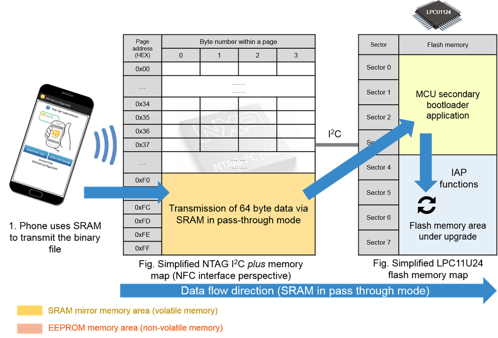
Regarding the NTAG I2C plus, it can be used as a bridge between NFC / I2C interfaces. The wireless firmware update consists of transferring the binary file to be flashed from one interface to the other. For transmission of large files, the NTAG I2C plus offers the pass-through mode, where the data is transferred using the 64 byte SRAM buffer. This buffer offers fast write access and unlimited write endurance as well as an easy handshake mechanism between the two interfaces. This buffer is mapped directly at the end of the Sector 0 of NTAG I2C plus (0x0F to 0xFF).
The data flow direction must be set with the TRANSFER_DIR session register. These pass-through direction settings avoid locking the memory access during the data transfer from one interface to the SRAM buffer. NTAG I2C plus introduces the FAST_READ command as FAST_WRITE command. With this new command, the whole SRAM can be written at once, which improves the total pass-through performance significantly. There is a dedicated application note detailing how to use the NTAG I2C plus for bidirectional communication http://www.nxp.com/documents/application_note/AN11579.pdf.
The wireless firmware update process goes as follows:
- The user selects from the phone application the binary file to be flashed. The phone splits the binary file in chunks of 64 bytes.
- With a tap, the phone writes 64 bytes in the SRAM. The MCU stores chunks of 64 bytes until it has one entire flash sector complete.
- Once a whole sector is received, the MCU executes the IAP functions to flash a memory sector
- This process is repeated until the whole binary file is transmitted
MCU / Embedded software integration
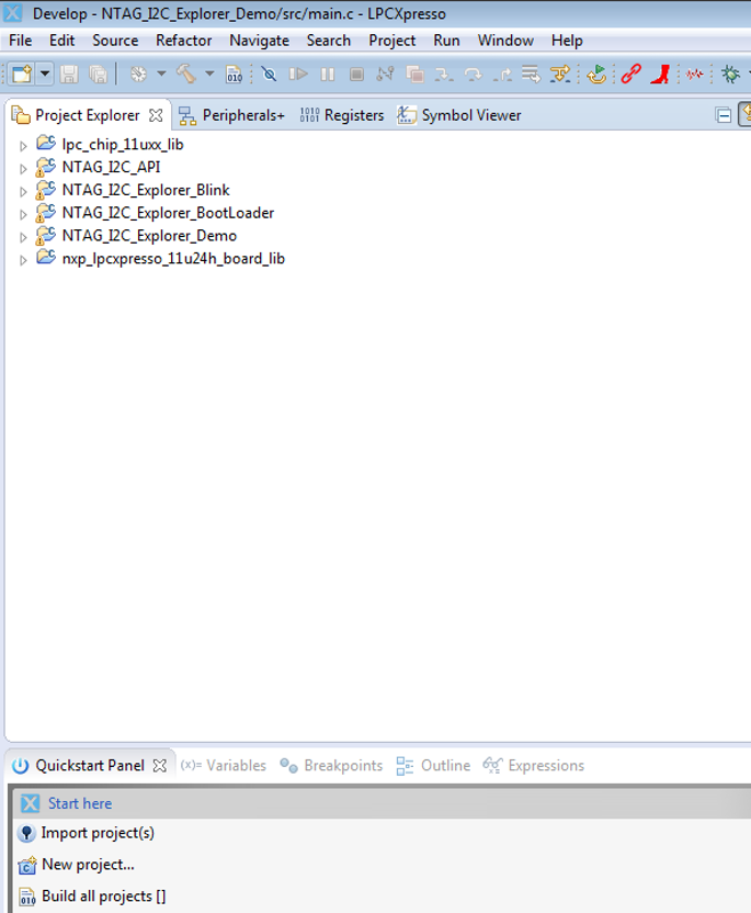
- The Lpc_chip_11uxx_lib and nxp_lpcxpresso_11u24h_board_lib project folders belong to the LPCOpen libraries supporting the LPC11U24 MCU and PCB board, the MCU chip integrated in the Explorer board. If you use another MCU, you should replace them by the specific LPCOpen libraries.
- The NTAG_I2C _API is a piece of code that provides a set of functions and procedures that allow you to communicate with the NTAG I2C from the I2C interface.
- The NTAG_Explorer_bootloader implements the secondary bootloader application we described previously. In this piece of code you will find the IAP functions implementation and the code handling SRAM data transfer.
And then, we include two end-user application examples:
- The NTAG_Explorer_demo, which implements the DIN module use cases
- The NTAG_Explorer_blink, which is a dummy application displaying a text message on the LCD when an RF field is detected. This application is provided to illustrate the NFC flashing functionality and its binary image is provided embedded by default into the Android app
NTAG_I2C_Explorer_bootloader application workflow
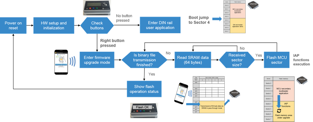
This is the first application executed when the Explorer board is powered up. Then, this application decides the next step:
- If the right button is not pressed, it jumps to sector 4 and executes the DIN module application.
- Otherwise, if the right button is pressed, it enters in firmware upgrade mode
As soon as the binary file is selected from the app, and we tap the phone, we start the transmission. The process goes as follows:
- The MCU reads chunks of 64 bytes of SRAM until a sector is received.
- Once a full sector is received, we flash an MCU sector using the IAP functions.
When the entire file in transmitted, the flash operation status is shown on the LCD and the MCU is reset so that the new binary file flash takes effect.
NTAG_I2C_Explorer_demo application workflow
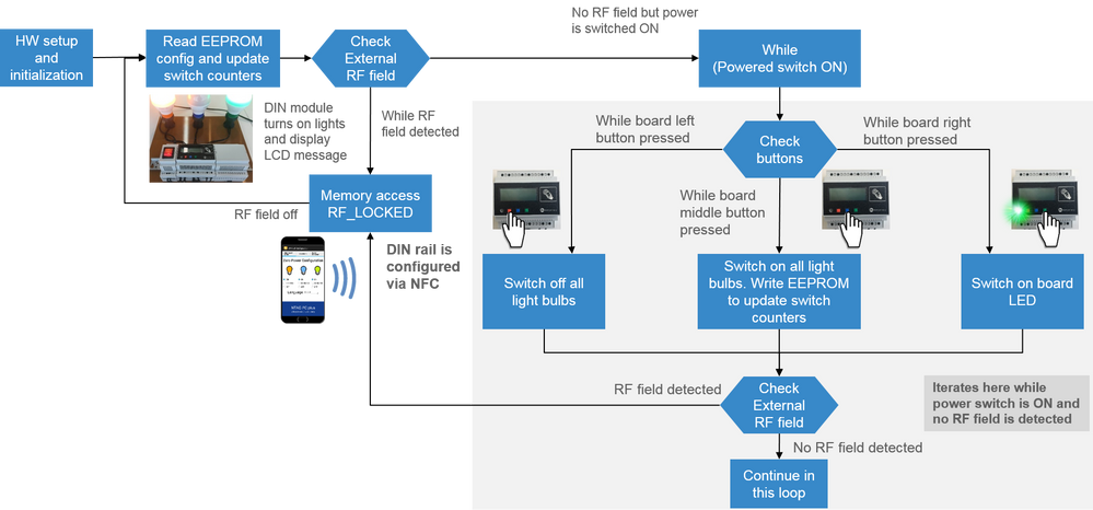
If the right button was not pressed, the NTAG_I2C_Explorer_demo application is executed. The first step executed by the MCU is to read the stored EEPROM configuration and apply these settings accordingly.Then, using a dedicated NTAG I2C plus register, it checks whether an RF field is present:
- If RF field is present, it means the user is currently configuring the DIN module. Thus, the memory access is locked so that the MCU cannot write on it. When the field is OFF, it means the user has finished the configuration. The MCU can read and apply the EEPROM settings once again.
- If there is no RF field present, the DIN module also allows a manual configuration using its buttons.
These manual button configurations perform the following actions:
- While the left button is pressed, all the GPIOs are set to low, so the light bulbs are switched OFF
- While the middle button is pressed, all the GPIOs are set to high, so the light bulbs are switched ON
- While the right button is pressed, the board LED is switched ON.
At any moment… if an RF field is detected, this loop is skipped and access to memory is locked for the I2C side since the user is configuring via the NFC interface
Phone / NFC device software integration

- All the NFC commands are implemented. So you can easily perform read / write operations using the READ/ WRITE and FAST READ / FAST WRITE commands. But also, the SECTOR_SELECT or PWD_AUTH
- Dedicated functions to READ / WRITE the registers
- Additional functions specially developed to make the read/write operations on SRAM easier.
NFC DIN rail Android demo application workflow
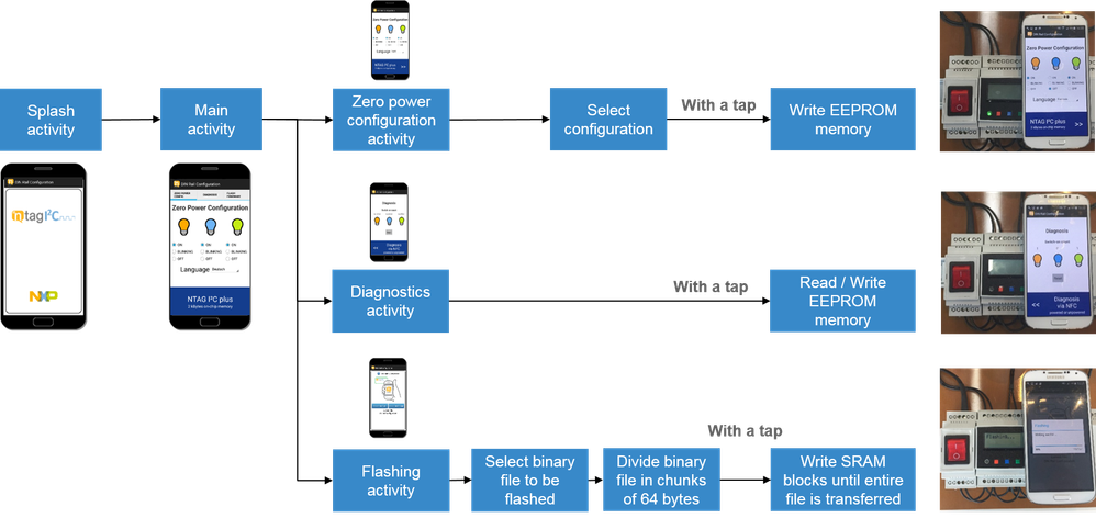
The Android phone application consists of a splash activity that leads us to a main activity with three tabs on the top side.
- If we keep the zero power configuration tab on, the desired settings can be selected. As soon as the phone is tapped, it executes a WRITE EEPROM command to save the configuration
- If we go to the diagnostics tab, a READ EEPROM operation is performed as soon as the phone is tapped. Or a WRITE EEPROM operation to overwrite the counters, if the reset button on the screen was pressed beforehand.
- Finally, if we go to the flash firmware tab, the binary file can be selected, and WRITE SRAM operations are used until the whole file has been transferred.
Video recorded session
On 21 February 2017, a live session explaining the NFC DIN rail demo was recorded. You can watch the recording here:
Available resources
I hope this entry has been useful. If you are interested in developing your own NFC solution, all the resources are available:
NTAG I2C plus Explorer kit
NTAG I2C plus Flex kit with additional antennas
Explorer board and Flex antenna HW design files
http://www.nxp.com/documents/software/SW3641.zip
http://www.nxp.com/documents/software/SW3639.zip
http://www.nxp.com/documents/software/SW3638.zip
NFC DIN module source code
http://nxp.com/assets/downloads/data/en/software/DINRailDemo_SourceCode.zip
NTAG I2C plus Explorer kit reference source code
