- Forums
- Product Forums
- General Purpose MicrocontrollersGeneral Purpose Microcontrollers
- i.MX Forumsi.MX Forums
- QorIQ Processing PlatformsQorIQ Processing Platforms
- Identification and SecurityIdentification and Security
- Power ManagementPower Management
- Wireless ConnectivityWireless Connectivity
- RFID / NFCRFID / NFC
- MCX Microcontrollers
- S32G
- S32K
- S32V
- MPC5xxx
- Other NXP Products
- S12 / MagniV Microcontrollers
- Powertrain and Electrification Analog Drivers
- Sensors
- Vybrid Processors
- Digital Signal Controllers
- 8-bit Microcontrollers
- ColdFire/68K Microcontrollers and Processors
- PowerQUICC Processors
- OSBDM and TBDML
- S32M
-
- Solution Forums
- Software Forums
- MCUXpresso Software and ToolsMCUXpresso Software and Tools
- CodeWarriorCodeWarrior
- MQX Software SolutionsMQX Software Solutions
- Model-Based Design Toolbox (MBDT)Model-Based Design Toolbox (MBDT)
- FreeMASTER
- eIQ Machine Learning Software
- Embedded Software and Tools Clinic
- S32 SDK
- S32 Design Studio
- GUI Guider
- Zephyr Project
- Voice Technology
- Application Software Packs
- Secure Provisioning SDK (SPSDK)
- Processor Expert Software
-
- Topics
- Mobile Robotics - Drones and RoversMobile Robotics - Drones and Rovers
- NXP Training ContentNXP Training Content
- University ProgramsUniversity Programs
- Rapid IoT
- NXP Designs
- SafeAssure-Community
- OSS Security & Maintenance
- Using Our Community
-
- Cloud Lab Forums
-
- Knowledge Bases
- ARM Microcontrollers
- i.MX Processors
- Identification and Security
- Model-Based Design Toolbox (MBDT)
- QorIQ Processing Platforms
- S32 Automotive Processing Platform
- Wireless Connectivity
- CodeWarrior
- MCUXpresso Suite of Software and Tools
- MQX Software Solutions
-
- Home
- :
- i.MX论坛
- :
- i.MX RT 交叉 MCU
- :
- Re: Preserving SNVS SRTC by connecting supercapacitor on VDD_SNVS_IN
Preserving SNVS SRTC by connecting supercapacitor on VDD_SNVS_IN
Preserving SNVS SRTC by connecting supercapacitor on VDD_SNVS_IN
Hello,
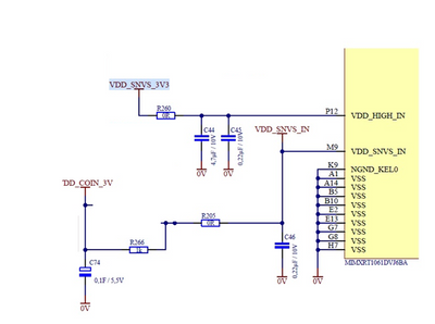
We have done a redesign of a formerly kinetis K61 based design. It this former design, we used a large capacitor (0.1F) to feed the VBAT voltage to the MCU according to the following schematic. With this design we could guarantee RTC retention and DRYICE storage for around 30 hours in the boards depending on tolerance on the C74 capacitor.
Having to do a redesign due to the lack of availability on the K61 processor, we have decided to proceed to a redesign based on the iMX RT MIMXRT1061 devices.
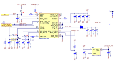
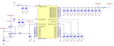
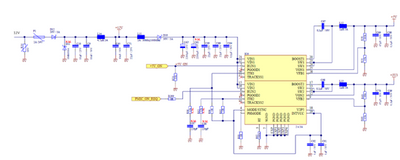
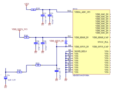
We have used a similar scheme in our MIMXRT1061 based design according to the following schematics trying to hold the SRTC and SNVS ZMK values for some time if the 12V voltage would have been dropped. The following schematics show the whole power supply related part of the design.
We know that the proper voltage range for the VDD_SNVS_IN is [2,4V ; 3,3V] to ensure the proper behavior of the RTC and LP register retention. From the Table 13 of the datasheet, we would expect that, if everything is shut, with C74 connected, the MCU would draw about 0.066 mW which would make about 30 minutes of data retention.
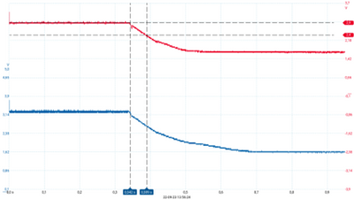
When we shut down the 12V external power supply and measure the voltage drop on VDD_SNVS_IN, we can observe a very quick and unexpected voltage drop below the 2.4V minimal voltage value avter about 50 ms.
So, here are my questions.
1. Can you figure out what we are we doing wrong in our design that might explain that the C74 capacitor does not hold enough energy to last more than 50 ms in the correct voltage range to ensure that RTC is correctly powered?
2. Would it be better that we connect the VDD_HIGH_IN input to our VDD_SNVS_3V3 source and keep the SVNS_VDD_IN connected to the capacitor? Table 3 of the datasheet and section 13.4.1.1.4 of the user manual seem to state that VDD_HIGH_IN might be used to charge the capacitor if the voltage of VDD_SVNS_IN is lower than the one of VDD_HIGH_IN. Should we keep the R266 resistor and what might be an appropriate value for a capacitor? I know that the documentation (Datasheets section 4.2.4.2) mentions computation for coin cell batteries but this might not be the case for supercapacitors.
3. Are there any specific register / fuse setup that should be enabled for RTC retention with battery / coin cell connected on VDD_SNVS_IN ?P
If VDD_SNVS_IN is directly supplied by a battery, a Schottky diode is required between VDD_HIGH_IN and VDD_SNVS_IN. The cathode is connected to VDD_SNVS_IN. Please make sure that your design is compatible with the hardware Development User Guide.
If using a battery then it is expected that it is exclusively connected to SNVS_IN.
Best regards,
Omar
Hello Omar,
Thanks for your reply and sorry for the delayed feedback.
Does that mean that the following schematic would be ok knowing that:
- VDD_SNVS_3V3 is a 3V3 power supply directly available as soon as the board is powered up.
- 3V3 is a 3V3 power supply generated by our step-down converter which is enabled only when PMIC-ON-REQ is correctly asserted by the CPU ?
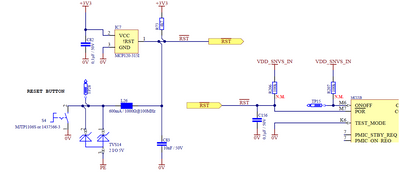
Knowing that we currently maintain a high level on ONOFF (M6) and POR_B (M7) through pull-ups connected to our VDD_SNVS_IN, would'nt it be better to feed those with VDD_SNVS_3V3 (which is connected to the VDD_HIGH_IN pin).
The current connections are as follows (I also added the schematics of the design part generating the RST_B signal through a button )
Note that these I/Os are associated with VDD_SNVS_IN (most inputs have on-chip pull resistors and do not require external resistors) Having resistors where not needed means higher current consumption. :
• PMIC_STBY_REQ—configurable output
• PMIC_ON_REQ—push-pull output
• TEST_MODE—on-chip pulldown
• WAKEUP—the GPIO that wakes the SoC up in the SNVS mode
The issue of using another source for pullup is that since they operate on SNVS domains, other voltage might interfere with the functions. Remember that SNVS is the first power domain to be powerup and the last one to power down.
• When VDD_SNVS_IN = VDD_HIGH_INin the SNVS domain, the current is drawn from both equally.
• When VDD_HIGH_IN > VDD_SNVS_IN, VDD_HIGH_IN supplies all the SNVS domain current and the current flows into VDD_SNVS_IN to charge the coin cell battery.
• When VDD_SNVS_IN > VDD_HIGH_IN, VDD_SNVS_IN supplies current to SNVS, and a small leakage current flows into VDD_HIGH_IN.

