- Forums
- Product Forums
- General Purpose MicrocontrollersGeneral Purpose Microcontrollers
- i.MX Forumsi.MX Forums
- QorIQ Processing PlatformsQorIQ Processing Platforms
- Identification and SecurityIdentification and Security
- Power ManagementPower Management
- MCX Microcontrollers
- S32G
- S32K
- S32V
- MPC5xxx
- Other NXP Products
- Wireless Connectivity
- S12 / MagniV Microcontrollers
- Powertrain and Electrification Analog Drivers
- Sensors
- Vybrid Processors
- Digital Signal Controllers
- 8-bit Microcontrollers
- ColdFire/68K Microcontrollers and Processors
- PowerQUICC Processors
- OSBDM and TBDML
- S32M
-
- Solution Forums
- Software Forums
- MCUXpresso Software and ToolsMCUXpresso Software and Tools
- CodeWarriorCodeWarrior
- MQX Software SolutionsMQX Software Solutions
- Model-Based Design Toolbox (MBDT)Model-Based Design Toolbox (MBDT)
- FreeMASTER
- eIQ Machine Learning Software
- Embedded Software and Tools Clinic
- S32 SDK
- S32 Design Studio
- GUI Guider
- Zephyr Project
- Voice Technology
- Application Software Packs
- Secure Provisioning SDK (SPSDK)
- Processor Expert Software
- MCUXpresso Training Hub
-
- Topics
- Mobile Robotics - Drones and RoversMobile Robotics - Drones and Rovers
- NXP Training ContentNXP Training Content
- University ProgramsUniversity Programs
- Rapid IoT
- NXP Designs
- SafeAssure-Community
- OSS Security & Maintenance
- Using Our Community
-
- Cloud Lab Forums
-
- Knowledge Bases
- ARM Microcontrollers
- i.MX Processors
- Identification and Security
- Model-Based Design Toolbox (MBDT)
- QorIQ Processing Platforms
- S32 Automotive Processing Platform
- Wireless Connectivity
- CodeWarrior
- MCUXpresso Suite of Software and Tools
- MQX Software Solutions
-
- Home
- :
- i.MXプロセッサ
- :
- i.MX RT Crossover MCUs Knowledge Base
- :
- RT1170 Octal flash enablement
RT1170 Octal flash enablement
- RSS フィードを購読する
- 新着としてマーク
- 既読としてマーク
- ブックマーク
- 購読
- 印刷用ページ
- 不適切なコンテンツを報告
RT1170 Octal flash enablement
RT1170 Octal flash enablement
RT1170 Octal flash enablement
1. Abstract
The MIMXRT1170-EVK hardware can directly support two types of flash: QSPI flash IS25WP128 and Octal flash MX25UM51345GXDI00. QSPI flash is used by default, so the FCB of the related SDK and some IDE debugger download flash drivers are also default to the QSPI flash. In practical usage, some customers need to use Octal flash with RT1170, but after modifying the EVK hardware to Octal flash MX25UM51345GXDI00, they may encounter various issues, such as download issues, boot issues, debug issues, and when the flash is empty or there is a valid boot code in the flash, the download result is different and so on.
This article will be based on NXP's official MIMXRT1170-EVK REV C1, modify the hardware onboard flash from QSPI flash to Octal flash MX25UM51345GXDI00, and modify the SDK project FCB, do ROM API test, do related tool download, do the debugger related flashloader modification and test with different IDE, so that customers who need it can refer to it. This article is not limited to EVK, but also applies to RT1170+Octal flash MX25UM51345GXDI00 with customer-defined board
Pic 1
2. Hardware modification
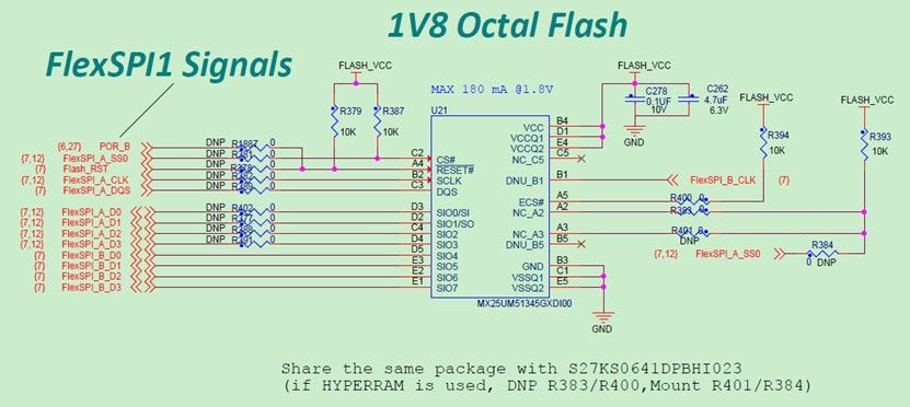
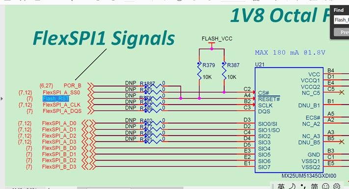
MIMXRT1170-EVK board modify flash to the octal flash, it needs to disconnect the QSPI flash pins, and connect the octal flash pins, the related modification points are:
OPTION2: USE Octal Flash( Mount R381/R378/R382/R389/R402/R377/R388/R391, DNP R380/R399/R386/R390/R392/R385)
Pic 2
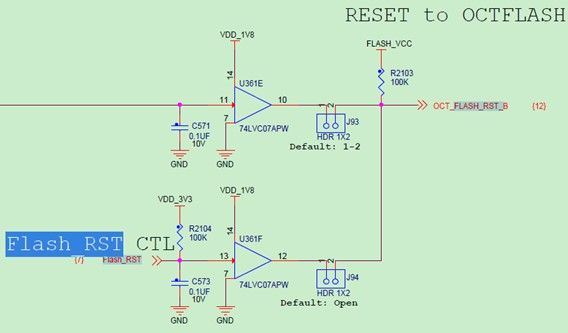
The octal flash BOOT_CFG pin configuration are as follows:
Pic 3
Pic 4
After modifying the hardware related resistors to choose the octal flash, SW1, SW2 should be configured to internal boot, and boot from octal flash, then it is controlled by the software part.
3. Octal flash APP FCB
3.1 Test SDK ROM API run from RAM
To verify the board hardware can run from the octal flash, we can test the SDK attached fsl_romapi project:
\SDK_2_12_0_MIMXRT1170-EVK\boards\evkmimxrt1170\driver_examples\fsl_romapi\cm7
Please note, can’t test the default project directly, as this project configuration is used by the QSPI flash, not the octal flash, if need to use the octal flash, customer need to modify the code at first, and add the GPIO to control the Flash_RST pin, which is used to reset the octal flash. The option0,1 value need to be modified to the octal flash values.
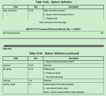
3.1.1 Octal flash option value
Pic 5
We can use the following option0 for testing, don’t need to configure the option1, as the octal flash is connected to the primary pin.
option0= 0Xc0400007, option1 = 0 //query_pad =1, cmd_pad=1,133MHz
option0= 0Xc0433007, option1 = 0 //query_pad =8, cmd_pad=8,133MHz
option0= 0Xc0403007, option1 = 0 //query_pad =1, cmd_pad=8,133MHz
3.1.2 fsl_romapi project testing
The modified code for the ROM API project are as follows, before call ROM_FLEXSPI_NorFlash_GetConfig API, it needs to use the GPIO to reset the external octal flash at first, so, here add the Flash_RST=GPIO_AD_03=GPIO09_IO02 pin GPIO configuration.
Pinmux.c related code:
gpio_pin_config_t gpio9_pinP15_config = {
      .direction = kGPIO_DigitalOutput,
      .outputLogic = 1U,
      .interruptMode = kGPIO_NoIntmode
  };
  GPIO_PinInit(GPIO9, 02U, &gpio9_pinP15_config);
  IOMUXC_SetPinMux(
	  IOMUXC_GPIO_AD_03_GPIO9_IO02,
      0U);
  IOMUXC_SetPinConfig(
	  IOMUXC_GPIO_AD_03_GPIO9_IO02,//OD,it is a workaround for EVK HW bug
	  0X12);
Flexspi_romapi.c added code:
static serial_nor_config_option_t option_1bit = {
    .option0.U = 0xc0400007U,
    .option1.U = 0U,
};
static serial_nor_config_option_t option_8bit = {
    .option0.U = 0xc0433007,
    .option1.U = 0U,
};
static serial_nor_config_option_t option_1_8bit = {
    .option0.U = 0xC0403007,
    .option1.U = 0U,
};
   GPIO_PinWrite(GPIO9, 02U, 0U);
	// Delay some time to reset external flash with Flash_RST pin
	for (uint32_t i = 0; i < 60000; i++)
		__asm volatile ("nop");
	GPIO_PinWrite(GPIO9, 02U, 1U);

    status = ROM_FLEXSPI_NorFlash_GetConfig(FlexSpiInstance, &norConfig, &option_8bit);
    if (status == kStatus_Success)
    {
        PRINTF("\r\n Successfully get FLEXSPI NOR configuration block with option_8bit\r\n ");
    }
    else
    {
        status = ROM_FLEXSPI_NorFlash_GetConfig(FlexSpiInstance, &norConfig, &option_1_8bit);
        if (status == kStatus_Success)
        {
            PRINTF("\r\n Successfully get FLEXSPI NOR configuration block with option_1_8bit\r\n ");
        }
        else
        {
            status = ROM_FLEXSPI_NorFlash_GetConfig(FlexSpiInstance, &norConfig, &option_1bit);
            if (status == kStatus_Success)
            {
              PRINTF("\r\n Successfully get FLEXSPI NOR configuration block with option_1bit\r\n ");
            }
            else
            {
              PRINTF("\r\n Get FLEXSPI NOR configuration block failure!\r\n");
              error_trap();
            }
        }
    }
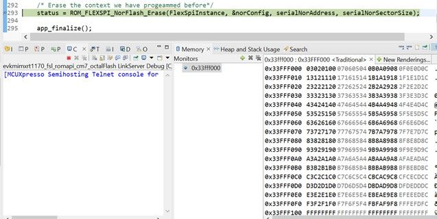
The test result is:
Pic 6
Pic 7
From the test result, we can see, after using the GPIO to reset the external flash, the practical used option value is:
option0= 0xc0403007, option1 = 0 //query_pad =1, cmd_pad=8,133MHz
It can read the SFDP successfully, get the flash config data to the norConfig, then use these values to configure the flexSPI module, at last, it realizes the octal flash related address area erase-write-read-erase operation.
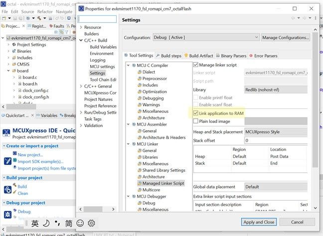
From the above test result, it means, the modified hardware is totally working. Please note, as we can’t confirm the external flash hardware is working, so this project FCB is still the default for the QSPI flash, not the octal flash, then when testing this fsl_romapi project, it’s better to run it from RAM not the external flash.
The following picture is how to run the project from the internal RAM, not download the flash directly:
Pic 8
Here, for the configuration, we also have one point that needs to note, why configure the GPIO pin Flash_RST: GPIO_AD_03 as OD(open drain)?
It is caused by the current MIMXRT1170-EVK hardware having a bug, so this OD configuration is used as the workaround. Octal flash MX25UM51345GXDI00 power supply voltage is 1.8V, but the GPIO_AD_03 bank voltage is 3.3V, between these two modules, no voltage convert hardware, so it will have the following situation:
a) Default GPIO_AD_03 is input mode, this pin has the internal PD(pull down) 35K resistor, and the external PU(pull up) 10K resistor to the 1.8V, Flash_RST=1.8V*35K/(10K+35K)=1.4V, this voltage also can be used as the enable signal.
To the normal boot, as the ROM didn’t control the octal flash Flash_RST pin, then this pin can be freely chose by any pin in the practical usage, so, the reset pin default is input, the voltage is 1.4V, it can enable the octal flash, no influence.
b) When need to control the octal flash reset, then it needs to use the GPIO control GPIO_AD_03 pin, if want to output 0, it is OK. But if want to output high level, use the internal PULL resistor, it will output 3.3V to the Flash_RST pin, this voltage already higher than the octal flash 1.8V, and the octal flash datasheet defines the max voltage is 2V, although the flash chip has the voltage buffer, input 3.3V in short time, won’t damage the chip, but after long time working, the chip normal working can’t be guaranteed, this will cause the risk. So, to solve this issues, we can do some workaround in the flashloader, rom API, when output the Flash_RST pin to higher, we can use OD mode, then the detail pin voltage is totally determined by the external pull circuit, and the EVK also have the external 10K PU to 1.8V, so it can output 1.8V not the 3.3V.
Pic 9
In the NXP new MIMXRT1170-EVKB board, the hardware adds the voltage convert chip to solve these issues, it can realize the 3.3V and 1.8V conversion:
Pic 10
3.2 MCUBootUtility program octal flash
We can use the MCUBootUtility to test MIMXRT1170-EVK+octal flash in serial download mode, normally for the chip connect, memory erase, read and program. This method also can use the tool to generated the correct FCB header for the octal flash, then can test the boot situation in the internal boot mode.
Serial download-> SW1:1-OFF,2-OFF,3-OFF,4-ON
Internal boot-> SW1:1-OFF,2-OFF,3-ON,4-OFF
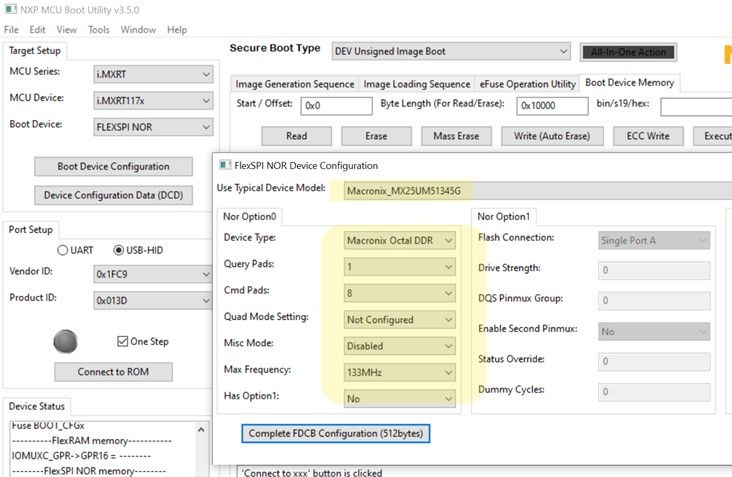
The MCUBootUtility configuration is:
Pic 11
This configuration is: option0=0Xc0403007,query 1wire, cmd 8 wire.
Then app image can use the MCUBootUtility attached code:
NXP-MCUBootUtility-3.5.0\apps\NXP_MIMXRT1170-EVK_Rev.A\cm7\led_blinky_0x3000a000.srec
Pic 12
We can see, the code downloading is finished, after this, reset device, configure the board as internal boot mode, then do the POR or the HW reset, we can see the on board LED D34 is blinking, it means the hardware also can boot from the octal flash.
3.3 SDK APP FDCB modification
If you need to debug the SDK APP demo from octal flash, you must ensure that the app correct FDCB is provided, then how to modify the app FDCB to octal flash? You can refer to the FDCB which is burned by the MCUBootUtility tool and the datasheet of the octal flash. Here is the FDCB that has been tested for many times. The key point is to provide the correct LUT table. Taking the RT1170 SDK led_blinky project as an example, the evkmimxrt1170_flexspi_nor_config.c file in the project xip file is modified as follows:
const flexspi_nor_config_t octalflash_config = {
    .memConfig =
        {
            .tag                 = FLEXSPI_CFG_BLK_TAG,
            .version             = FLEXSPI_CFG_BLK_VERSION,
            .readSampleClksrc=kFlexSPIReadSampleClk_ExternalInputFromDqsPad,
            .csHoldTime          = 3,
            .csSetupTime         = 3,
            .deviceModeCfgEnable = 1,
            .deviceModeType      = kDeviceConfigCmdType_Spi2Xpi,
            .waitTimeCfgCommands = 1,
            .deviceModeSeq =
                {
                    .seqNum   = 1,
                    .seqId    = 6, /* See Lookup table for more details */
                    .reserved = 0,
                },
            .deviceModeArg = 2, /* Enable OPI DDR mode */
            .controllerMiscOption =
                (1u << kFlexSpiMiscOffset_SafeConfigFreqEnable) | (1u << kFlexSpiMiscOffset_DdrModeEnable),
            .deviceType    = kFlexSpiDeviceType_SerialNOR,
            .sflashPadType = kSerialFlash_8Pads,
            .serialClkFreq = kFlexSpiSerialClk_133MHz,
            .sflashA1Size  = 64ul * 1024u * 1024u,
            .dataValidTime =
                {
                    [0] = {.time_100ps = 16},
                },
            .busyOffset      = 0u,
            .busyBitPolarity = 0u,
            .lookupTable =
                {
                		/* Read */// EEH+11H+32bit addr+20dummy cycles+ 4Bytes read data    //133Mhz 20 dummy=10+10
                		[0 + 0] = FLEXSPI_LUT_SEQ(CMD_DDR  , FLEXSPI_8PAD, 0xEE, CMD_DDR, FLEXSPI_8PAD, 0x11),//0x871187ee,
                		[0 + 1] = FLEXSPI_LUT_SEQ(RADDR_DDR, FLEXSPI_8PAD, 0x20, DUMMY_DDR, FLEXSPI_8PAD, 0x0A),//0xb30a8b20,
                		[0 + 2] = FLEXSPI_LUT_SEQ(DUMMY_DDR, FLEXSPI_8PAD, 0x0A, READ_DDR, FLEXSPI_8PAD, 0x04),//0xa704b30a,

						/* Read Status SPI */// SPI 05h+ status data 0X24 maybe 0X04
                		[4*1 + 0] = FLEXSPI_LUT_SEQ(CMD_SDR  , FLEXSPI_1PAD, 0x05, READ_SDR, FLEXSPI_1PAD, 0x24),//0x24040405,

						/* Read Status OPI *///05H+FAH+ 4byte 00H(addr)+4Byte read
                		[4*2 + 0] = FLEXSPI_LUT_SEQ(CMD_DDR  , FLEXSPI_8PAD, 0x05, CMD_DDR, FLEXSPI_8PAD, 0xFA),//0x87fa8705,
                		[4*2 + 1] = FLEXSPI_LUT_SEQ(CMD_DDR  , FLEXSPI_8PAD, 0x00, CMD_DDR, FLEXSPI_8PAD, 0x00),//0x87008700,
                		[4*2 + 2] = FLEXSPI_LUT_SEQ(CMD_DDR  , FLEXSPI_8PAD, 0x00, CMD_DDR, FLEXSPI_8PAD, 0x00),//0x87008700,
                		[4*2 + 3] = FLEXSPI_LUT_SEQ(READ_DDR  , FLEXSPI_8PAD, 0x04, STOP_EXE, FLEXSPI_1PAD, 0x00),//0x0000a704,

						/* Write enable SPI *///06h
                		[4*3 + 0] = FLEXSPI_LUT_SEQ(CMD_SDR  , FLEXSPI_1PAD, 0x06, STOP_EXE, FLEXSPI_1PAD, 0x00),//0x00000406,

						/* Write enable OPI *///06h+F9H
                		[4*4 + 0] = FLEXSPI_LUT_SEQ(CMD_DDR  , FLEXSPI_8PAD, 0x06, CMD_DDR, FLEXSPI_8PAD, 0xF9),//0x87f98706,

						/* Erase sector */ //21H+DEH + 32bit address
                		[4*5 + 0] = FLEXSPI_LUT_SEQ(CMD_DDR  , FLEXSPI_8PAD, 0x21, CMD_DDR, FLEXSPI_8PAD, 0xDE),//0x87de8721,
                		[4*5 + 1] = FLEXSPI_LUT_SEQ(RADDR_DDR  , FLEXSPI_8PAD, 0x20, STOP_EXE, FLEXSPI_1PAD, 0x00),//0x00008b20,

                        /*Write Configuration Register 2 =01, Enable OPI DDR mode*/ //72H +32bit address + CR20x00000000 = 0x01
                		[4*6 + 0] = FLEXSPI_LUT_SEQ(CMD_SDR  , FLEXSPI_1PAD, 0x72, CMD_SDR, FLEXSPI_1PAD, 0x00),//0x04000472,
                		[4*6 + 1] = FLEXSPI_LUT_SEQ(CMD_SDR  , FLEXSPI_1PAD, 0x00, CMD_SDR, FLEXSPI_1PAD, 0x00),//0x04000400,
                		[4*6 + 2] = FLEXSPI_LUT_SEQ(CMD_SDR  , FLEXSPI_1PAD, 0x00, WRITE_SDR, FLEXSPI_1PAD, 0x01),//0x20010400,

						/*block erase*/ //DCH+23H+32bit address
                		[4*8 + 0] = FLEXSPI_LUT_SEQ(CMD_DDR  , FLEXSPI_8PAD, 0xDC, CMD_DDR, FLEXSPI_8PAD, 0x23),//0x872387dc,
                		[4*8 + 1] = FLEXSPI_LUT_SEQ(RADDR_DDR, FLEXSPI_8PAD, 0x20, STOP_EXE, FLEXSPI_1PAD, 0x00),//0x00008b20,

						/*page program*/ //12H+EDH+32bit address+ write data 4bytes
                		[4*9 + 0] = FLEXSPI_LUT_SEQ(CMD_DDR  , FLEXSPI_8PAD, 0x12, CMD_DDR, FLEXSPI_8PAD, 0xED),//0x87ed8712,
                		[4*9 + 1] = FLEXSPI_LUT_SEQ(RADDR_DDR, FLEXSPI_8PAD, 0x20, WRITE_DDR, FLEXSPI_8PAD, 0x04),//0xa3048b20,

						/* Chip Erase (CE) Sequence *///60H+9FH
                		[4*11 + 0] = FLEXSPI_LUT_SEQ(CMD_DDR  , FLEXSPI_8PAD, 0x60, CMD_DDR, FLEXSPI_8PAD, 0x9F),//0x879f8760,
                },
        },
    .pageSize           = 256u,
    .sectorSize         = 4u * 1024u,
    .blockSize          = 64u * 1024u,
    .isUniformBlockSize = false,
};
The LUT here is the full function LUT table, it includes: 8 wire read, 1/8 wire status read, 1/8 wire write enable, 8 wire sector erase, 1 wire write configuration enable for OPI DDR mode, 8 wire block erase, 8 wire page program, 8 wire chip erase. The detail command is the same as the MX25UM51345GXDI00 datasheet, and also the same as the MCUBootUtility tool generated FCB.
4. CMSIS DAP Flashloader
MIMXRT1170-EVK default use the CMSIS DAP debugger, take the MCUXPresso IDE as an example, it will call the flashloader named as .cfx file, flashloader source code can be found from this path:
C:\nxp\MCUXpressoIDE_11.6.0_8187\ide\Examples\Flashdrivers\NXP\iMXRT\ iMXRT117x_FlexSPI_SFDP.zip
The exist .cfx file which can be used directly, the path is:
C:\nxp\MCUXpressoIDE_11.6.0_8187\ide\binaries\Flash\
MIMXRT1170_SFDP_QSPI.cfx: QSPI flash
MIMXRT1170_SFDP_MXIC_OPI.cfx: octal flash
Pic 13
When use flashloader + CMSIS DAP + MCUXpresso debug result is:
Pic 14
One point need to note, mcuxpresso IDE flashloader source code iMXRT117x_FlexSPI_SFDP.zip, the project configured to the octal flash, the related Flash_RST control code need to be modified, otherwise, when it output high, the voltage will be 3.3V.
Pic 15
In the above picture,
add code:
MEM_WriteU32(0x400E835CU, 0x12);
Which is SW_PAD_CTL_PAD_GPIO_AD_03 register = 0x12, OD mode, then generate the mxic MX25UM51345GXDI00 octal flash .cfx file again, which is used for the mcuxpresso+CMSIS DAP debugger.
5. JLINK Flashloader with RT-UFL
In actual use, many customers not only use the on-board CMSIS-DAP debugger, but also like to use external JLINK/JLINK plus, or use the on-board JLINK firmware (use LPCScrypt modify firmware, pay attention to update the JINK firmware according to the instructions on the webpage), or use the external JLINK firmware (need to disconnect the onboard debugger jumper). But if the JLINK flash driver is called directly, it will be QSPI flash. Here is how to use the flash driver of the octal flash in JLINK. Now the JLINK driver uses JLinkARM.dll to define the flash used by different chips, unlike the old JLINK driver. The firmware of the flash is called by JLinkDevices.xml. The .dll file cannot allow users to directly modify the corresponding flash of the device, so it is necessary to provide a flash driver file that supports RT1170 octal flash, and add a calling command in JLinkDevices.xml to override the default QSPI definition in JLinkARM.dll.
NXP AE has developed a very useful full-function flash driver called RT-UFL, which can support general QSPI, hyperflash, octaflash, etc. Users can use JLINK to call RT-UFL flash driver, and then use JFLASH, JLINK commander, or IDE (MCUXpresso, IAR, MDK) to realize the debugging and downloading of RT chips combined with different flashes
RT-UFL download link:
https://github.com/JayHeng/RT-UFL
More detail usage of RT-UFL, please check this blog link:
https://www.cnblogs.com/henjay724/
After downloading, install the RT-UFL to the JLINK driver, copy the following folder file:
RT-UFL-1.0\algo\SEGGER\JLink_Vxxx
to the JLINK driver install path:
C:\Program Files\SEGGER\JLINKV768B
The JLINK driver link is:
https://www.segger.com/downloads/jlink/JLink_Windows_x86_64.exe
Now, use the original RT-UFL firmware combined with JFLASH to test the octal flash in RT1170 directly, and the debugger is JLINK plus, just to check whether it can be run, device selection: MIMXRT1170_UFL_L0.
_L0 suffix algorithm is suitable for QSPI Flash and Octal Flash (Page size is 256 Bytes, Sector size is 4KB), _L1/2 suffix algorithm is suitable for Hyper Flash (Page size is 512 Bytes, Sector size is 4KB/64KB).
5.1 RT-UFL JFlash Test
Generate a .srec file for the led_blinky project which FCB has been modified to octal flash before, it will be used by JFLASH or JLINK commander later.
Use JFLASH combined with JLINK plus to create a new JFLASH project. The chip is selected as MIMXRT1170_UFL_L0 which can support octal flash.
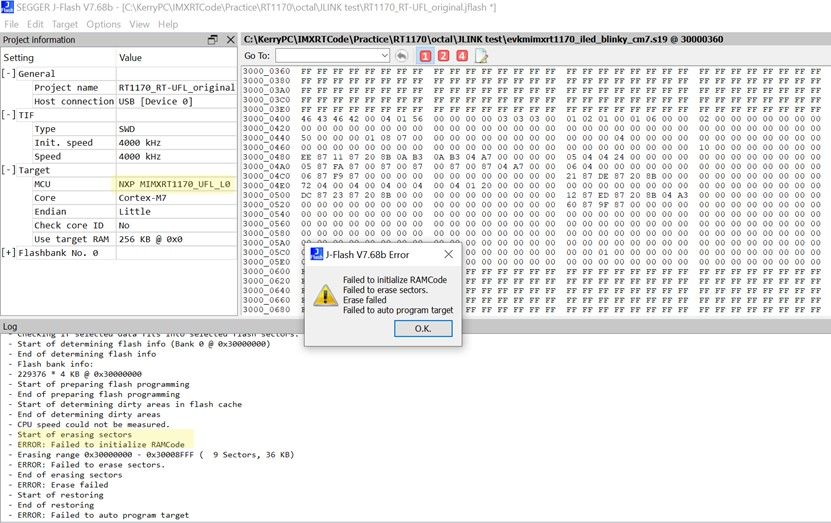
The test situation is as follows, you can see that the connect can be successful, and the ARM CortexM7 core can be found, but the programming, reading, and erasing functions will fail. It can be said that the connection to the external octal flash is not successful at all:
Pic 16
If the used JLINK is not the JLINK plus, due to the license can’t support the JFLASH, then customer can use the JLINK commander to test it, but here, the test result with the original RT-UFL is totally the same as the JFLASH:
Pic 17
It can still meet the issues of “Failed to initialize RAMCode”, even use the mem32 readout the address data, sometimes, the data is not correct, not the real flash data, customer can compare the memory which the data which is readout from the MCUBootUtility.
So, the RT-UFL flashdriver code need to be modified to the octal flash, to let the octal flash works.
5.2 RT-UFL Flashloader source code modification
From the analysis of the original RT-UFL combined with the octal flash test, after many modifications and tests, the modification points are listed one by one, the new flashloader file generated by the modified RT-UFL is tested using JFlash, JLINK commander, IDE, etc. JLINK tools are divided into external JLINK plus and onboard JLINK firmware (JFLASH is not supported).
5.2.1 Flashloader modification points
1) RAMCode errors
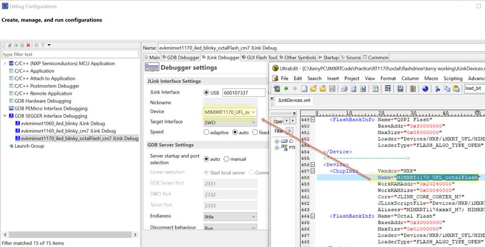
In the JLinkDevices.xml file, define the RAM location to the OCRAM address:
 <Device>
    <ChipInfo      Vendor="NXP"
                   Name="MIMXRT1170_UFL_octalFlash"
                   WorkRAMAddr="0x20240000"
                   WorkRAMSize="0x00040000"
                   Core="JLINK_CORE_CORTEX_M7"
                   JLinkScriptFile="Devices/NXP/iMXRT_UFL/iMXRT117x_CortexM7.JLinkScript"
                   Aliases="MIMXRT1176xxx8_M7; MIMXRT1176xxxA_M7" />
    <FlashBankInfo Name="Octal Flash"
                   BaseAddr="0x30000000"
                   MaxSize="0x01000000"
                   Loader="Devices/NXP/iMXRT_UFL/MIMXRT_FLEXSPI_UV5_UFL.FLM"
                   LoaderType="FLASH_ALGO_TYPE_OPEN" />
  </Device>
2) Add erase sector ROM API
The JLINK calls the erase sector, so add the related sector erase API:
ufl_main.c
static void ufl_fill_flash_api(void)
{
...
        case kChipId_RT117x:
            uflTargetDesc->flashDriver.init      = g_bootloaderTree_imxrt117x->flexspiNorDriver->init;
            uflTargetDesc->flashDriver.page_program= g_bootloaderTree_imxrt117x->flexspiNorDriver->page_program;
            uflTargetDesc->isFlashPageProgram           = true;
            uflTargetDesc->flashDriver.erase_all = g_bootloaderTree_imxrt117x->flexspiNorDriver->erase_all;
            uflTargetDesc->flashDriver.erase = g_bootloaderTree_imxrt117x->flexspiNorDriver->erase;
		uflTargetDesc->flashDriver.erase_sector= g_bootloaderTree_imxrt117x->flexspiNorDriver->erase_sector;//kerry add
 		uflTargetDesc->flashDriver.read = g_bootloaderTree_imxrt117x->flexspiNorDriver->read;
            uflTargetDesc->flashDriver.set_clock_source = NULL;
            uflTargetDesc->flashDriver.get_config= g_bootloaderTree_imxrt117x->flexspiNorDriver->get_config;
               uflTargetDesc->iarCfg.enablePageSizeOverride = true;
            break;
…
}
ufl_flexspi_nor_flash_imxrt117x.h
typedef struct _flexspi_nor_flash_driver_imxrt117x
{
    uint32_t version;
    status_t (*init)(uint32_t instance, flexspi_nor_config_t *config);
    status_t (*page_program)(uint32_t instance, flexspi_nor_config_t *config, uint32_t dst_addr, const uint32_t *src);
    status_t (*erase_all)(uint32_t instance, flexspi_nor_config_t *config);
    status_t (*erase)(uint32_t instance, flexspi_nor_config_t *config, uint32_t start, uint32_t lengthInBytes);
    status_t (*read)(uint32_t instance, flexspi_nor_config_t *config, uint32_t *dst, uint32_t addr, uint32_t lengthInBytes);
    void (*clear_cache)(uint32_t instance);
    status_t (*xfer)(uint32_t instance, flexspi_xfer_t *xfer);
    status_t (*update_lut)(uint32_t instance, uint32_t seqIndex, const uint32_t *lutBase, uint32_t seqNumber);
    status_t (*get_config)(uint32_t instance, flexspi_nor_config_t *config, serial_nor_config_option_t *option);
    status_t (*erase_sector)(uint32_t instance, flexspi_nor_config_t *config, uint32_t address);//kerry add
    status_t (*erase_block)(uint32_t instance, flexspi_nor_config_t *config, uint32_t address);
    const uint32_t reserved0;
    status_t (*wait_busy)(uint32_t instance, flexspi_nor_config_t *config, bool isParallelMode, uint32_t address);
    const uint32_t reserved1[2];
} flexspi_nor_flash_driver_imxrt117x_t;
3) Speed up the erase and program speed
FlashDev.c
struct FlashDevice const FlashDevice = {
   FLASH_DRV_VERS,             // Driver Version, do not modify!
   "MIMXRT_FLEXSPI_RT1170",           // Device Name
   EXTSPI,                     // Device Type
   0x30000000,                 // Device Start Address
   0x01000000,                 // Device Size in Bytes (16mB)
   256*4,                        // Programming Page Size
   0,                          // Reserved, must be 0
   0xFF,                       // Initial Content of Erased Memory
   100,                        // Program Page Timeout 100 mSec
   15000,                      // Erase Sector Timeout 15000 mSec

   // Specify Size and Address of Sectors
   4096*8, 0x00000000,         // Sector Size  4kB (256 Sectors)
   SECTOR_END
};
FlashPrg.c:
int EraseSector (unsigned long adr) {

    uint32_t instance = g_uflTargetDesc.flexspiInstance;
    uint32_t baseAddr = g_uflTargetDesc.flashBaseAddr;
    /*Erase Sector*/
    status_t status =  flexspi_nor_flash_erase(instance, (void *)&flashConfig, adr - baseAddr, FLASH_DRV_SECTOR_SIZE*8);//kerry *8, 4096
    if (status != kStatus_Success)
    {
        return (1);
    }
    else
    {
        return (0);
    }
}

int ProgramPage (unsigned long adr, unsigned long sz, unsigned char *buf) {

    status_t status = kStatus_Success;
    uint32_t instance = g_uflTargetDesc.flexspiInstance;
    uint32_t baseAddr = g_uflTargetDesc.flashBaseAddr;
    uint32_t loadaddr = adr - baseAddr;
    unsigned char *buffer;
    buffer = buf;
    int i;
    for(i = 0; i < 4; i ++) // kerry add 256*4
    {
        status =  flexspi_nor_flash_page_program(instance, (void *)&flashConfig, loadaddr, (uint32_t *)buffer);
        if (status != kStatus_Success)
        {
            return (1);
        }
        buffer+=256;
        loadaddr+=256;
    }

    return (0);
}
The principle is to reduce the times it takes for the PC to send commands to JLINK and then send to the board, now, one command can directly erase and program multiple blocks.
4) Octal Flash option value polling
It should be noted that after Flash Reset, or the first programming, it is necessary to read SFDP in a single-line manner. If it is not reset and there is a valid FCB in the flash, the flash is initialized to OPT mode and needs to be read in 8-line mode. At this time, the valid SFDP table of the flash chip cannot be read in the single-line mode.
RT-UFL is a flashloader that supports multiple chips, and it does not use specific GPIO as the chip flash_RST. For RT-UFL, GPIO is not added to control flash_RST pin, and a large degree of freedom is reserved. Otherwise, once the customer uses the RST pins that are different from EVK still have problems, and even require customers to spend time modifying the flashloader source code, increasing development time.
Therefore, in view of the above considerations, modify the code here, do not add RESET signal control, do not fix option value for single-line or 8-line, but polling the option with single-line and 8-line to read SPDF.
ufl_main.c
static void ufl_set_target_property(void)
    case kChipId_RT117x:
            uflTargetDesc->flexspiInstance = MIMXRT117X_1st_FLEXSPI_INSTANCE;
            uflTargetDesc->flexspiBaseAddr = MIMXRT117X_1st_FLEXSPI_BASE;
            uflTargetDesc->flashBaseAddr   = MIMXRT117X_1st_FLEXSPI_AMBA_BASE;
           // uflTargetDesc->configOption.option0.U = 0xc0433007;
           // uflTargetDesc->configOption.option1.U = 0x0;
            break;
Make sure that the above option are not configured, otherwise the option configuration will be fixed and the polling option function will no longer be enabled.
ufl_auto_probe_flash.c
static const serial_nor_config_option_t s_flashConfigOpt[] = {
		 // 1st Pinmux, PortA for octal 1 bit SFDP for no FCB in flash eg. MX25UM51345G
           {.option0.U = 0xc0403007, .option1.U = 0x00000000},
		 // 1st Pinmux, PortA for octal 8 bit SFDP for FCB in flash eg. MX25UM51345G
		{.option0.U = 0xc0433007, .option1.U = 0x00000000},
           // 1st Pinmux, PortA for octal 1 bit SFDP &1 bit CMD for no FCB in flash eg. MX25UM51345G
		{.option0.U = 0xc0400007, .option1.U = 0x00000000},
..}
After the above modifications, compile the source code project of RT-UFL:
RT-UFL-1.0\build\mdk\MIMXRT_FLEXSPI_UV5.uvprojx,
Generate a new MIMXRT_FLEXSPI_UV5_UFL.FLM programming algorithm and copy it to the following path:
C:\Program Files\SEGGER\JLINKV768B\Devices\NXP\iMXRT_UFL
The device name defined in JLinkDevices.xml is: MIMXRT1170_UFL_octalFlash.
JLinkDevices.xml path:
C:\Program Files\SEGGER\JLINKV768B
modify the .xml, and add the above-mentioned "RAMCode error" section.
After the modification is completed, refresh the JLinkDLLUpdater.exe file, so that several IDEs can synchronize the firmware defined by the updated xml file.
5.2.2 JFlash Test
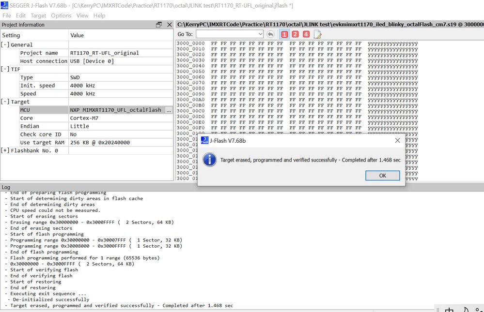
As can be seen from the test results of Jflash below, it can be successfully erased, and the app image can be downloaded to octal flash. After the download is successful, reset it, and you can see the onboard led is flashing. It shows that the modified RT-UFL flashloader has worked. It should be noted here that the use of JFLASH requires the use of an external Segger JLINK Plus. Some customers use normal JLINK or RT EVK onboard JLINK firmware, then they can try the JLINK commander method.
Pic 18
5.2.3 JLINK command Test
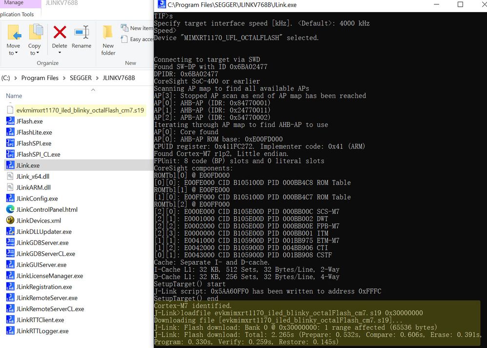
Use the JLINK plus associated with JLINK commander test result is:
Pic 19
You can see that the firmware can be downloaded successfully.
Now uses the EVK onboard JLINK firmware to test as follows, it can be seen that the programming is normal, so if users don’t have external JLINK can also directly use the RT EVK onboard JLINK firmware. One thing need to pay attention to is when using the onboard JLINK firmware, the firmware will cause the debugger port USB to not directly supply power to the RT chip, so it needs to be configured that J38 is connected to 3-4, and then find another USB cable to connect J20 to supply power to the board.
Pic 20
5.3 MCUXpresso + JLINK +Modified RT-UFL Testing
At first, select the MCUXPresso IDE JLINK debug path, add the JLINK driver path which is already added RT-UFL firmware, windows->preferences, then the path should like this:
Pic 21
When downloading, still need to configure RUN->Debugger configurations, the JLINK configuration should be:
Pic 22
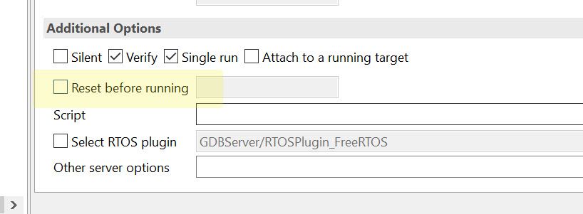
Please note, don’t check the item “Reset before running” in the debug configuration, as this item is checked in default.
Pic 23
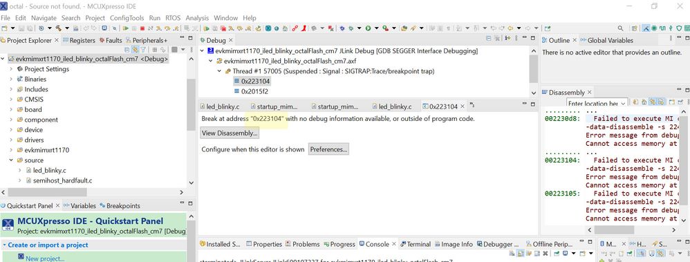
If checked “Reset before running”, when debug it, the code will be blocked after downloading the code, and can’t jump to the main function. If customer click halt button, it will meet the issues that the code is stop at 0x223104, but after exit the debug mode, and do the POR again, you will find the flash already downloaded with the app successfully.
Pic 24
This problem is related to the impact of RT1170 security policy on JLINK. For details, please refer to the following link:
https://www.cnblogs.com/henjay724/p/15725966.html
When JLink is connected to the chip, as long as the reset command is executed, it will directly enter the safe debugging mode (the PC stops at 0x223104).
Therefore, make sure that "Reset before running" is not checked, so that you can enter the debug and main functions normally, and the test results are as follows:
Pic 25
5.4 MDK+JLINK+Modified RT-UFLTesting
Next, use the MCUXPresso CFG tool combined with the SDK package to export an MDK project, also based on the led_blinky project, and modify the FCB code for Octal flash, and then call the modified RT-UFL flashloader, the device name is: MIMXRT1170_UFL_octalFlash.
Note, be sure to refresh:
C:\Program Files\SEGGER\JLINKV768B\JLinkDLLUpdater.exe
Make sure the IDE is using the latest firmware link.
The following is a specific MDK project related configuration pictures:
Pic 26
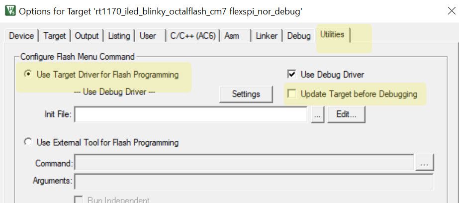
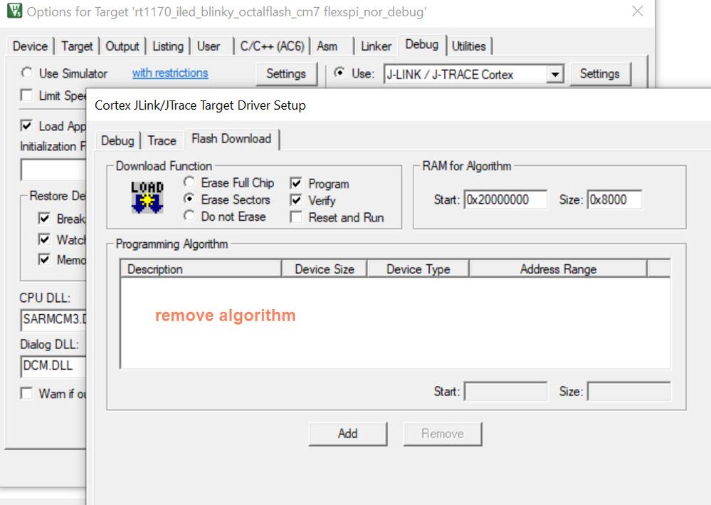
The project is selected as flexspi_nor_debug, and after compiling, the debug tool is configured as JLINK, the JLINK simulation sequence can be found, and the updated target before debugging in utilities should not be checked:
Pic 27
Pic 28
Pic 29
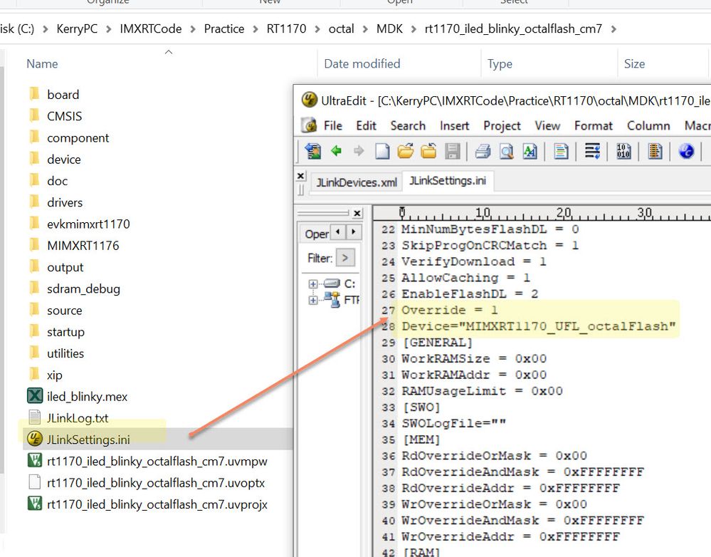
Modify JlinkSettings.ini,configure override =1, device as the RT-UFL modified firmware device name: MIMXRT1170_UFL_octalFlash.
Pic 30
Pic 31
As can be seen from the above picture, the modified RT-UFL Octal flash has been successfully used to run the MDK project.
It should be noted that do not use the download button, because this button cannot use the overwritten and modified RT-UFL programming algorithm, it will still call the programming algorithm of the deleted area of the interface, and an error will be reported if it cannot be found.
5.5 IAR + JLINK + Modified RT-UFL Testing
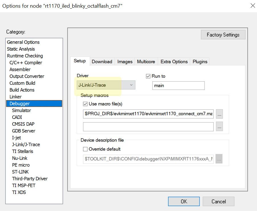
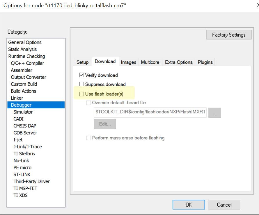
Here is the use of IAR combined with JLINK to debug RT1170 octal flash, using the modified RT-UFL programming algorithm. The specific configuration is as follows:
Pic 32
Don’t check “use flash loaders”, it means don’t use the IAR attached .out download algorithm, and use the JLINK driver’s modified RT-UFL octal flash flashdriver.
Pic 33
Reset can choose core, if it is normal, debug will meet the same issues with the MCUXPresso which checked reset item, PC will stop to 0x223104.
Pic 34
Here, modify project settings folder ->.jlink file, use the RT-UFL device name: MIMXRT1170_UFL_octalFlash,
And override =1, then it will call the modified RT-UFL flashloader. If you can’t find the .jlink in the new created project, just select the JLINK debugger, click download at first, then it will generate the .jlink file, then modify it and debug it again.
Pic 35
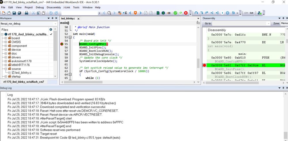
After modify the RT-UFL program algorithm to the octal flash, click “download and debug” button, it will enter the debug mode, in the following picture, the code is running successfully:
Pic 36
6. Conclusion
After the above details, the code download of the MIMXRT1170-EVK on-board octalflash can be realized, and the fsl_romspi project is used to run in RAM, which can verify the normal reading and writing of the hardware octalflash, and MCUBootutility to verify the programming and boot conditions. The modification of APP FCB is matched octal flash. The debugger uses JLINK or CMSIS DAP, and the correct flashdriver programming algorithm needs to be used. In particular, JLINK needs to use the RT-UFL as flashloader, but the source code needs to be modified. Finally, you can see that the combination of RT-UFL download algorithm and JLINK, successfully realize the download and operation of octal flash code on MCUXpresso, IAR, MDK three IDEs. This article is not limited to MIMXRT1170-EVK, but also applies to customer design boards using RT1170+ MX25UM51345GXDI00 octal flash.
The attachment adds the modified RT-UFL programming algorithm and the octal flash project of the three major IDEs.

