- Forums
- Product Forums
- General Purpose MicrocontrollersGeneral Purpose Microcontrollers
- i.MX Forumsi.MX Forums
- QorIQ Processing PlatformsQorIQ Processing Platforms
- Identification and SecurityIdentification and Security
- Power ManagementPower Management
- MCX Microcontrollers
- S32G
- S32K
- S32V
- MPC5xxx
- Other NXP Products
- Wireless Connectivity
- S12 / MagniV Microcontrollers
- Powertrain and Electrification Analog Drivers
- Sensors
- Vybrid Processors
- Digital Signal Controllers
- 8-bit Microcontrollers
- ColdFire/68K Microcontrollers and Processors
- PowerQUICC Processors
- OSBDM and TBDML
- S32M
-
- Solution Forums
- Software Forums
- MCUXpresso Software and ToolsMCUXpresso Software and Tools
- CodeWarriorCodeWarrior
- MQX Software SolutionsMQX Software Solutions
- Model-Based Design Toolbox (MBDT)Model-Based Design Toolbox (MBDT)
- FreeMASTER
- eIQ Machine Learning Software
- Embedded Software and Tools Clinic
- S32 SDK
- S32 Design Studio
- GUI Guider
- Zephyr Project
- Voice Technology
- Application Software Packs
- Secure Provisioning SDK (SPSDK)
- Processor Expert Software
- MCUXpresso Training Hub
-
- Topics
- Mobile Robotics - Drones and RoversMobile Robotics - Drones and Rovers
- NXP Training ContentNXP Training Content
- University ProgramsUniversity Programs
- Rapid IoT
- NXP Designs
- SafeAssure-Community
- OSS Security & Maintenance
- Using Our Community
-
- Cloud Lab Forums
-
- Knowledge Bases
- ARM Microcontrollers
- i.MX Processors
- Identification and Security
- Model-Based Design Toolbox (MBDT)
- QorIQ Processing Platforms
- S32 Automotive Processing Platform
- Wireless Connectivity
- CodeWarrior
- MCUXpresso Suite of Software and Tools
- MQX Software Solutions
-
- Home
- :
- i.MX フォーラム
- :
- i.MXプロセッサ
- :
- imx6 board ddr
imx6 board ddr
- RSS フィードを購読する
- トピックを新着としてマーク
- トピックを既読としてマーク
- このトピックを現在のユーザーにフロートします
- ブックマーク
- 購読
- ミュート
- 印刷用ページ
imx6 board ddr
- 新着としてマーク
- ブックマーク
- 購読
- ミュート
- RSS フィードを購読する
- ハイライト
- 印刷
- 不適切なコンテンツを報告
NXP's imx6 development board's DDR layout does not conform to the 3W principle, the spacing between lines is only 4mil.doesn't the board work well?
- 新着としてマーク
- ブックマーク
- 購読
- ミュート
- RSS フィードを購読する
- ハイライト
- 印刷
- 不適切なコンテンツを報告
Hello jinyi7016,
Would you please provide more information as for what i.MX6 board are you referring to?
The recommendations for Hardware Design for the i.MX6 are on the following document:
https://www.nxp.com/docs/en/user-guide/IMX6DQ6SDLHDG.pdf
From this document clocks or strobes that are on the same layer need at least 2.5× spacing from an adjacent trace (2.5× height from reference plane) to reduce cross-talk. NXP boards should have this spacing albeit not in all DDR signals but rather on clocks and strobe signals.
Regards,
- 新着としてマーク
- ブックマーク
- 購読
- ミュート
- RSS フィードを購読する
- ハイライト
- 印刷
- 不適切なコンテンツを報告
Thanks Reply
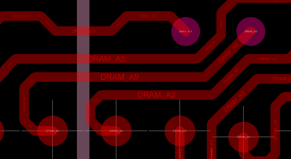
this board is mx6 dual lite sabre ai cpu card.
As the showed picture,the width of DRAM_A5,A9,A2 is 4.7mil,but the spacing of net A5,A9,A2 is 4mil ,does it OK for DDR?
there is other designs ,every net's sapcing is the 3X of the Cline width.Is it necessary?
- 新着としてマーク
- ブックマーク
- 購読
- ミュート
- RSS フィードを購読する
- ハイライト
- 印刷
- 不適切なコンテンツを報告
Hello jinyi7016,
It is desirable to follow the 3W rule in all signals, if possible. However, sometimes this is impossible due to space constraints. In those scenarios the absolutely critical signals are clocks and strobes which should at least have 2.5X spacing.
The design looks okay. However, I would recommend giving as much space as possible and testing it after manufacturing. In the final product the manufacturing variations will also affect the design and it's there where you would need to make sure that the DDR works properly. There is a Stress Tool that will surely help:
i.MX6/7 DDR Stress Test Tool V2.92
Regards,
