- Forums
- Product Forums
- General Purpose MicrocontrollersGeneral Purpose Microcontrollers
- i.MX Forumsi.MX Forums
- QorIQ Processing PlatformsQorIQ Processing Platforms
- Identification and SecurityIdentification and Security
- Power ManagementPower Management
- Wireless ConnectivityWireless Connectivity
- RFID / NFCRFID / NFC
- MCX Microcontrollers
- S32G
- S32K
- S32V
- MPC5xxx
- Other NXP Products
- S12 / MagniV Microcontrollers
- Powertrain and Electrification Analog Drivers
- Sensors
- Vybrid Processors
- Digital Signal Controllers
- 8-bit Microcontrollers
- ColdFire/68K Microcontrollers and Processors
- PowerQUICC Processors
- OSBDM and TBDML
- S32M
-
- Solution Forums
- Software Forums
- MCUXpresso Software and ToolsMCUXpresso Software and Tools
- CodeWarriorCodeWarrior
- MQX Software SolutionsMQX Software Solutions
- Model-Based Design Toolbox (MBDT)Model-Based Design Toolbox (MBDT)
- FreeMASTER
- eIQ Machine Learning Software
- Embedded Software and Tools Clinic
- S32 SDK
- S32 Design Studio
- GUI Guider
- Zephyr Project
- Voice Technology
- Application Software Packs
- Secure Provisioning SDK (SPSDK)
- Processor Expert Software
-
- Topics
- Mobile Robotics - Drones and RoversMobile Robotics - Drones and Rovers
- NXP Training ContentNXP Training Content
- University ProgramsUniversity Programs
- Rapid IoT
- NXP Designs
- SafeAssure-Community
- OSS Security & Maintenance
- Using Our Community
-
- Cloud Lab Forums
-
- Knowledge Bases
- ARM Microcontrollers
- i.MX Processors
- Identification and Security
- Model-Based Design Toolbox (MBDT)
- QorIQ Processing Platforms
- S32 Automotive Processing Platform
- Wireless Connectivity
- CodeWarrior
- MCUXpresso Suite of Software and Tools
- MQX Software Solutions
-
Hello everybody,
I'm new to the community and I have a question about audio interface of DeltaSigma converters with i.MX6 processor.
For my application, I need the following configuration, that should work in Synchronous mode:
- N°3 I2S output lines
- N°2 I2S input lines
to interace with the i.MX6 Audio Section.
Is it possible to achiev this goal by ESAI interface?
If i.MX6 should be the Master, what i.MX6 line must be used as Master Clock?
Thank you in advance for you reply.
Best Regards,
Diego Ferraiuolo
已解决! 转到解答。
Hi Every one,
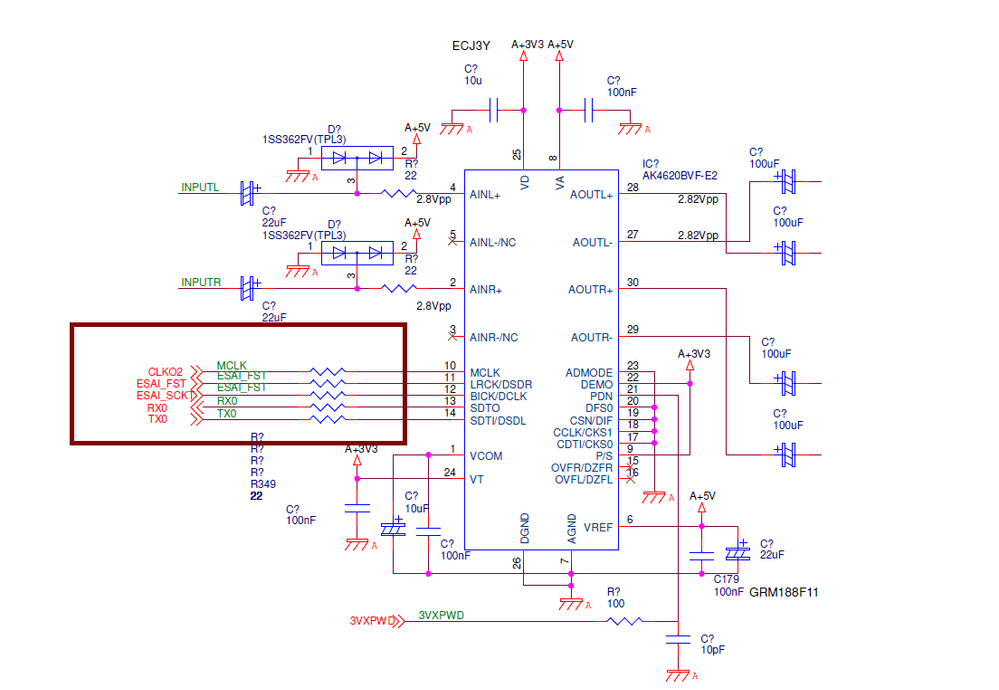
May I seek yours help to share below is correct connection for ESAI/TDM interface for audio path
I have connect this to NXP DSP IC
The BGA pad number/name all is under GPIO for IMX6
regards
Mun Ei
Hi diego
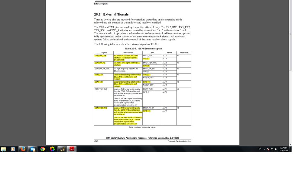
I think this is possible. For ESAI signals please look at
Table 25-1. ESAI External Signals IMX6DQRM
example connections: SCH-26662_e.pdf p.5
bare metal software examples
i.MX 6Series Platform SDK  : Bare-metal SDK
iMX6_Firmware_Guide.pdf sect.9.1 ESAI overview
Best regards
igor
-----------------------------------------------------------------------------------------------------------------------
Note: If this post answers your question, please click the Correct Answer button. Thank you!
-----------------------------------------------------------------------------------------------------------------------
Dear Igor,
thank you so much for your prompt and clear suggestions.
I would like to ask you, please, something else:
-Is it possible to connect,in the same way the ESAI CODEC is connected, separate CODECS and DACS?
I ask you because I would like to use CODEC from AKM like the AK4621 with a higher Dynamic Range (in this case 115dB).
In my application, for handling the N°3 I2S Output Lines and the N°2 I2S Input LinesI would use 2 Codecs (AK4621) and one DAC (AAK4382).
-The Master Clock, if generated internally, should be passed in Input to the i.MX6 processor too?
Are these pins CLK2_N and CLK2_P?
-If pins CLK2_N and CLK2_P are routed out of the System On Module, is it better to use the Master Clock
internally generated from i.MX6?
Thank you again.
Best Regards,
Diego
Hi Diego
I had worked on a design for a client where we had 3 codecs
connected to ESAI ports. We used two separate set of ESAI_SCKR,
ESAI_FSR, ESAI_HCKR and ESAI_RXD/TXD. We used ADIO_PLL
based generated clock according to that Clock Generator Functional
Block Diagram Igor has referred to. Unfortunately I don't have access
to this design any more but hopefully this info will be of some help to you.
Regards
Sinan Akman
Hi Diego
ESAI has independent (asynchronous mode) or shared (synchronous mode)
transmitter and receiver sections, up to six transmitters and four receivers
with TX2_RX3, TX3_RX2, TX4_RX1, and TX5_RX0 pins shared by transmitters
2 to 5 and receivers 0 to 3.
Synchronous or asynchronous, that is, the transmitter and receiver sections
may use common clock and synchronization signals (synchronous operating mode),
or they may have their own separate clock and sync signals (asynchronous operating mode).
Regarding "Master Clock", suggest to look at Table 25-2 ., Table 25-3 IMX6DQRM
Figure 25-32. ESAI Clock Generator Functional Block Diagram
ESAI system clock, (esai_clk_root or EXTAL) can be outputted on CLKO pins with register
CCM_CCOSR , sect.18.6.21 CCM Clock Output Source Register (CCM_CCOSR) IMX6DQRM
I do not think that CLK2_N and CLK2_P can be used as master clock, its options are given in
LVDS2_CLK_SEL, sect.50.7.6 Miscellaneous Register 1 (PMU_MISC1n).
~igor
Dear Igor,
thank you for your reply.
You are very kind and very helpful.
So I understand that I can use separate Codecs and Dacs,
but if all of them have to operate in synchronous mode,
should I use SCKR, FSR for the receiver section (ADC)
and SCKT, FST for the transmitter section (DAC), or have I to use only
two of them?
I ask you because in the standard Codecs, a DAC and an ADC are on the same Chip,
but there is only 1 SCK line, 1 FS line, 1 MCLK line in addition to the SDI and SDO lines.
For the system clock (Master Clock) I understand I have to select
CLKO pins by register CCM_CCOSR. Do you refer to CCM_CLKO1 and CCM_CLKO2?
Which pin should be used as Master Clock?
Before I told you about pins CLK2_N and CLK2_P,
as I looked to them at page 7 of the schematic sch-27767_a_x3.pdf
in the directory SABRE-AI_DualLite_CPUcard.
How it is used the Audio Oscillator ?
Thank you very much.
Best Regards.
Diego
Hi Diego
for connections one can look at Sabre-AI CS42888 codec, it also has
DAC and an ADC are on the same chip
CS42888 SCH-26662 p.5 i.MX6_SABRE_AI_DESIGNFILES
ESAI system clock, (esai_clk_root or EXTAL) can be outputted on CLKO2,
selection of CLKO2_SEL.
Regarding "Audio Oscillator", Y1 is used for external
ESAI_SSI_EXT1_CLK, not for i.MX6.
~igor
Hi Igor,
I have looked at the SCH-2662_e.pdf page 5.
The ESAI CODEC has 2 sections:
one for ADC and it uses the following signals :ESAI_SCKR, ESAI_FSR, RX0, RX1
and one for DAC where the following signals are involved: ESAI_SCKT, ESAI_FST, TX0,TX1,TX2,TX3
I think it works in Asynchronous mode. Am I wrong?
Or if it is working in Synchronous Mode SCKT=SCKR and FST=FSR?
If I have a standard I2S Codec with an ADC and a DAC and only 3 clock lines, i.e. 1xSCK 1xFS and 1x MCLK,
and if I have to work in Synchronous Mode and the i.MX6 as Master,
should I use for that signal lines
SCKT for SCK
FST for FS
CLKO2 for MCLK
to drive my CODEC Clock Lines?
Thank you so much!!
Diego.
Hi Diego
there is no way to input external master clock as clocks
Fsys = ipg_clk_esai, EXTAL=esai_clk_root
generated internally, shown on Table 25-3 IMX6DQRM
Figure 25-32. ESAI Clock Generator Functional Block Diagram.
~igor
~igor
Hi Igor,
I have a doubt.
Ok, Fsys = ipg_clk_esai, EXTAL=esai_clk_root are generated internally,
and they are the source clocks for the ESAI Clock Generator (Figure 25-32).
At page 1231 of IMX6DQRM you can read:
25.2.11 High Frequency Clock for Transmitter
.................................................................................
In the synchronous mode (SYN=1), it operates as the high frequency clock input or output used by all enabled transmitters and
receivers.
.................................................................................
When programmed as output it can serve as a high frequency sample clock (to external DACs
for example) or as an additional system clock (see Table 25-3).
So it seems that HCKT should be used as Master Clock for the Codecs.
HCKT should be the ESAI_TX_HF_CLK available to the pin GPIO_4 in mode ALT0.
Am I wrong? What do you think about?
I understand that I can output the ESAI System Clock (esai_clk_root or EXTAL) on CLKO pins with register CCM_CCOSR,
but I have the doubt that the ESAI System Clock (esai_clk_root or EXTAL) is the MCLK to be passed to the CODECS.
Please, let me understand.
Thank you, again.
Best Regards,
Diego
Hi Diego.
answer depends on what do you mean by
"Master Clock for the Codecs". Actually
Figure 25-32. ESAI Clock Generator Functional Block Diagram
shows all clock generation.
Best regards
igor

