- Forums
- Product Forums
- General Purpose MicrocontrollersGeneral Purpose Microcontrollers
- i.MX Forumsi.MX Forums
- QorIQ Processing PlatformsQorIQ Processing Platforms
- Identification and SecurityIdentification and Security
- Power ManagementPower Management
- MCX Microcontrollers
- S32G
- S32K
- S32V
- MPC5xxx
- Other NXP Products
- Wireless Connectivity
- S12 / MagniV Microcontrollers
- Powertrain and Electrification Analog Drivers
- Sensors
- Vybrid Processors
- Digital Signal Controllers
- 8-bit Microcontrollers
- ColdFire/68K Microcontrollers and Processors
- PowerQUICC Processors
- OSBDM and TBDML
- S32M
-
- Solution Forums
- Software Forums
- MCUXpresso Software and ToolsMCUXpresso Software and Tools
- CodeWarriorCodeWarrior
- MQX Software SolutionsMQX Software Solutions
- Model-Based Design Toolbox (MBDT)Model-Based Design Toolbox (MBDT)
- FreeMASTER
- eIQ Machine Learning Software
- Embedded Software and Tools Clinic
- S32 SDK
- S32 Design Studio
- GUI Guider
- Zephyr Project
- Voice Technology
- Application Software Packs
- Secure Provisioning SDK (SPSDK)
- Processor Expert Software
-
- Topics
- Mobile Robotics - Drones and RoversMobile Robotics - Drones and Rovers
- NXP Training ContentNXP Training Content
- University ProgramsUniversity Programs
- Rapid IoT
- NXP Designs
- SafeAssure-Community
- OSS Security & Maintenance
- Using Our Community
-
- Cloud Lab Forums
-
- Knowledge Bases
- ARM Microcontrollers
- i.MX Processors
- Identification and Security
- Model-Based Design Toolbox (MBDT)
- QorIQ Processing Platforms
- S32 Automotive Processing Platform
- Wireless Connectivity
- CodeWarrior
- MCUXpresso Suite of Software and Tools
- MQX Software Solutions
-
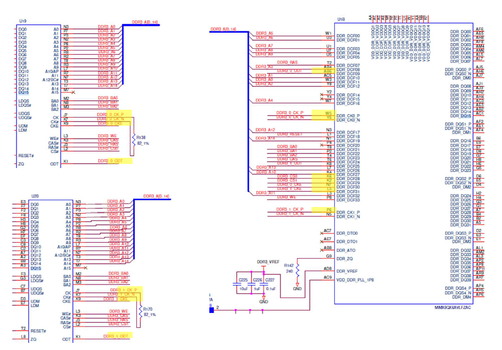
I design circuit boad including I.MX8QXP and two DDR3Ls.
And I have a question about pin assignment of I.MX8QXP.
I.MX8QXP: MIMX8QX6AVLFZAC
DDR3L: 256M x 16 (M41K256M16TW)
Q.1
Which pin assignment is correct using I.MX8QXP and two DDR3Ls?
Assigmnet A:
<From DQ0 to DQ15>
ODT0 AB6
CK0P W5
CK0N Y6
CKE0 N7
CS0 K6
<From DQ16 to 31>
ODT1 K8
CK1P P6
CK1N N5
CKE1 L5
CS1 K2
<Common connection : From DQ0 to DQ15 and from DQ16 to DQ31>
ODT AB6
CKP W5
CKN Y6
CKE N7
CS K6
ODT1 K8 (NC)
CK1P P6 (NC)
CK1N N5 (NC)
CKE1 L5 (NC)
CS1 K2 (NC)
Q2.
I want to know about data swapping of i.MX8QXP.
Is there any problem if the pins are replaced on the i.MX8QXP side and DDR3L side within each byte?
Thanks
Takahashi
已解决! 转到解答。
Hello,
1. The correct DDR3L interface signal interconnection table is as shown below.
i.MX8QXP 1st DDR3L chip
DQ[15:0] DQ[15:0]
ODT0 AB6 ODT
CK0P W5 CK_P
CK0N Y6 CK_N
CKE0 N7 CKE
CS0 K6 CS
i.MX8QXP 2nd DDR3L chip
DQ[31:16] DQ[15:0]
ODT0 AB6 ODT
CK0P W5 CK_P
CK0N Y6 CK_N
CKE0 N7 CKE
CS0 K6 CS
I.e. the same clock/clock enable/chip select/ODT signals should be used for both DDR3L chips. Is it what you mean as your Assignment B? If so, it is correct.
2. It's OK to swap data bits within the same byte lane (but not across the byte lanes).
Best Regards,
Artur
