- Forums
- Product Forums
- General Purpose MicrocontrollersGeneral Purpose Microcontrollers
- i.MX Forumsi.MX Forums
- QorIQ Processing PlatformsQorIQ Processing Platforms
- Identification and SecurityIdentification and Security
- Power ManagementPower Management
- MCX Microcontrollers
- S32G
- S32K
- S32V
- MPC5xxx
- Other NXP Products
- Wireless Connectivity
- S12 / MagniV Microcontrollers
- Powertrain and Electrification Analog Drivers
- Sensors
- Vybrid Processors
- Digital Signal Controllers
- 8-bit Microcontrollers
- ColdFire/68K Microcontrollers and Processors
- PowerQUICC Processors
- OSBDM and TBDML
- S32M
-
- Solution Forums
- Software Forums
- MCUXpresso Software and ToolsMCUXpresso Software and Tools
- CodeWarriorCodeWarrior
- MQX Software SolutionsMQX Software Solutions
- Model-Based Design Toolbox (MBDT)Model-Based Design Toolbox (MBDT)
- FreeMASTER
- eIQ Machine Learning Software
- Embedded Software and Tools Clinic
- S32 SDK
- S32 Design Studio
- GUI Guider
- Zephyr Project
- Voice Technology
- Application Software Packs
- Secure Provisioning SDK (SPSDK)
- Processor Expert Software
- MCUXpresso Training Hub
-
- Topics
- Mobile Robotics - Drones and RoversMobile Robotics - Drones and Rovers
- NXP Training ContentNXP Training Content
- University ProgramsUniversity Programs
- Rapid IoT
- NXP Designs
- SafeAssure-Community
- OSS Security & Maintenance
- Using Our Community
-
- Cloud Lab Forums
-
- Knowledge Bases
- ARM Microcontrollers
- i.MX Processors
- Identification and Security
- Model-Based Design Toolbox (MBDT)
- QorIQ Processing Platforms
- S32 Automotive Processing Platform
- Wireless Connectivity
- CodeWarrior
- MCUXpresso Suite of Software and Tools
- MQX Software Solutions
-
- Home
- :
- i.MX フォーラム
- :
- i.MXプロセッサ
- :
- Re: PMIC coltages
PMIC coltages
- RSS フィードを購読する
- トピックを新着としてマーク
- トピックを既読としてマーク
- このトピックを現在のユーザーにフロートします
- ブックマーク
- 購読
- ミュート
- 印刷用ページ
PMIC coltages
- 新着としてマーク
- ブックマーク
- 購読
- ミュート
- RSS フィードを購読する
- ハイライト
- 印刷
- 不適切なコンテンツを報告
Hi,
I have drawn the schematic of i.MX6UL and PF3000(PMIC), by taking reference from Freescale EVK.
However now at the output of front end LDO, I am getting 3.4V, which should be 4.4V typical.
This net name mentioned as SYS_4V4 in the schematic.
There is 470pF capacitor between Source and Gate and I am getting 5V at both the ends.
Could you please help us on this issue at the earliest.
Regards,
Surendra
- 新着としてマーク
- ブックマーク
- 購読
- ミュート
- RSS フィードを購読する
- ハイライト
- 印刷
- 不適切なコンテンツを報告
Hello Surendra,
Can you please try the following,
1.- Select in the boot config pins the value to Boot from eMMC. Try to measure that the pin values are correct and the fuses for boot options are correct.
2.- Measure the signals of the eMMC, let´s said clock signal, just to make sure the device it is trying to find the image from this location. if you see activity in the clock that means the i.MX it is trying to boot but the image it is not correct or in the wrong place.
3.- If the signal activity it is not working, verify in the console that the fuse are correct, and try again.
Have a great day,
TIC
-----------------------------------------------------------------------------------------------------------------------
Note: If this post answers your question, please click the Correct Answer button. Thank you!
-----------------------------------------------------------------------------------------------------------------------
- 新着としてマーク
- ブックマーク
- 購読
- ミュート
- RSS フィードを購読する
- ハイライト
- 印刷
- 不適切なコンテンツを報告
Hello Surendra,
As you can see in the reference manual, in the Boot Section, if the CPU does not found the Booting Image ( let´s said bootloader) the system automatically, change to another boot option, until get in the Serial Boot Mode.
Hope this helps
Have a great day,
TIC
-----------------------------------------------------------------------------------------------------------------------
Note: If this post answers your question, please click the Correct Answer button. Thank you!
-----------------------------------------------------------------------------------------------------------------------
- 新着としてマーク
- ブックマーク
- 購読
- ミュート
- RSS フィードを購読する
- ハイライト
- 印刷
- 不適切なコンテンツを報告
Hi,
But when board is in serial download mode, we get information on console that image is properly stored in eMMC & when we switch to internal boot mode, it doesn't execute through eMMC.
Regards,
Surendra
- 新着としてマーク
- ブックマーク
- 購読
- ミュート
- RSS フィードを購読する
- ハイライト
- 印刷
- 不適切なコンテンツを報告
Hi Jose,
We have progressed on i.MX6UL testing. We have one issue.
Initially we have made BOOT_CFG (1) : 0 & BOOT_CFG (0) : 1 to keep CPU in serial boot mode & tested DDR3, also stored boot image in eMMC through USB.
After this we did BOOT_CFG (1) : 1 &BOOT_CFG (0) : 0 to keep CPU in internal boot mode to execute image through eMMC.
However, despite of above change, CPU remains in serial boot mode. Can you guide me what could be reason that is keeping CPU in serial boot mode.
Regards,
Surendra.
- 新着としてマーク
- ブックマーク
- 購読
- ミュート
- RSS フィードを購読する
- ハイライト
- 印刷
- 不適切なコンテンツを報告
Hi,
Adding one more thing that we have made proper setting of BOOT_CFG pins through resistors to set boot option as eMMC.
Regards,
Surendra.
- 新着としてマーク
- ブックマーク
- 購読
- ミュート
- RSS フィードを購読する
- ハイライト
- 印刷
- 不適切なコンテンツを報告
Dear Jose,
As I explained above that we are getting all the output voltages after bringing PMIC out from Standby mode.
We have not connected i.MX6UL CPU yet to PMIC.
Now when we are testing the various power rails of PMIC output, we are facing one common issue on all power output rails.
If we are testing SW1A (DCDC_3V3) with load, we find the voltage as 3.25V and we also find voltage dip to 0V on this rail.
The dip duration is 16 msec to 18 msec and duration between two consecutive dips is approx. 4.88 msec.
The same observed on other 3.3V rails such as SW2 (VPERI_3V3), V33(VDD_HIGH_IN) etc.
The same is being observed on rails other than 3.3V such SW1B (VDD_ARM_SOC_IN) 1.4V (dipping to 0V),
SWBST (DRAM_1V35) 1.35V (dipping to 0V). The dipping rate is approx. 4.88 sec between two dips.
This is happening at any current even from 100mA to max load current rail can deliver.
If we are observing such a behaviour then we can connect PMIC output to CPU as it may lead to resetting of CPU.
Can you please help us to resolve above issue. What could be probable reason for such voltage dips in regulator outputs.
Dear Jose,
I would like to make one more rquest to you that, can you help us by giving some other faster mode of communication,
as your solution we are checking next day and things are getting delayed.
Best Regards,
Surendra
- 新着としてマーク
- ブックマーク
- 購読
- ミュート
- RSS フィードを購読する
- ハイライト
- 印刷
- 不適切なコンテンツを報告
Dear Surendra,
As I explained above that we are getting all the output voltages after bringing PMIC out from Standby mode.
[Answer] It shows that PMIC power up is OK.
We have not connected i.MX6UL CPU yet to PMIC.
Now when we are testing the various power rails of PMIC output, we are facing one common issue on all power output rails.
If we are testing SW1A (DCDC_3V3) with load, we find the voltage as 3.25V and we also find voltage dip to 0V on this rail.
The dip duration is 16 msec to 18 msec and duration between two consecutive dips is approx. 4.88 msec.
The same observed on other 3.3V rails such as SW2 (VPERI_3V3), V33(VDD_HIGH_IN) etc.
The same is being observed on rails other than 3.3V such SW1B (VDD_ARM_SOC_IN) 1.4V (dipping to 0V),
SWBST (DRAM_1V35) 1.35V (dipping to 0V). The dipping rate is approx. 4.88 sec between two dips.
This is happening at any current even from 100mA to max load current rail can deliver.
[Answer] Please double check the Standby pin status during customer’s test. If it’s in Standby mode, the front-end LDO is max 1.0mA current capability. I judge that the problem is coming from the current limit of the front-end LDO, you can bypass the external PMOS circuit, and directly supply 4.0V to VIN(pin #42) to try these regulator’s output with some loadings again. Please note that the regulators: VCC_SD, V33 and SWBST are coming from VIN2(pin #38).
Regards,
Jose
- 新着としてマーク
- ブックマーク
- 購読
- ミュート
- RSS フィードを購読する
- ハイライト
- 印刷
- 不適切なコンテンツを報告
Dear Jose,
We have checked the supply rails by removing front end LDO, however we are observing the same issue of voltage dips after 5 sec.
So it seems its not related to this.
I am doubting on SNVS_PMIC_ON_REQ (Bal T9 of CPU), as per datasheet it has to driven to Power on PMIC.
Currently we have not powered CPU and this unpowered ball is driving this pin.
The other way I think is, it needs external button input to Power on the PMIC.
There are three modes also inside the PMIC which gets enabled sequentially and during this period we may see voltage variations in the output.
Can this be one of the reason for voltage dips?
Regards,
Surendra
- 新着としてマーク
- ブックマーク
- 購読
- ミュート
- RSS フィードを購読する
- ハイライト
- 印刷
- 不適切なコンテンツを報告
Dear Jose,
One more observation is that we are exactly pulses on PWRON pin with 5 sec delay between two consecutive pulses (Standby is pulled down by 10K and its low all the time, while PWRON pulled up but still we find pulses).
This time is exactly same the way we are getting voltage dips.
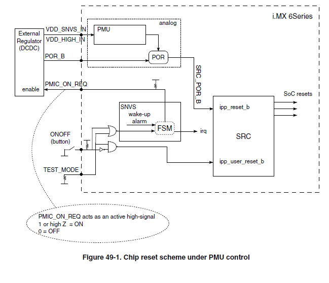
Do you suggest us to power VDD_SNVS_IN and VDD_HIGH_IN supply to CPU as below(i.MX6UL reference manual).
I think connecting VDD_SNVS_IN and VDD_HIGH_IN rails shall not affect or damage the CPU and CPU can take care of the PWRON and Standby pins.
Regards,
Surendra
- 新着としてマーク
- ブックマーク
- 購読
- ミュート
- RSS フィードを購読する
- ハイライト
- 印刷
- 不適切なコンテンツを報告
Hi Surendra,
One more observation is that we are exactly pulses on PWRON pin with 5 sec delay between two consecutive pulses (Standby is pulled down by 10K and its low all the time, while PWRON pulled up but still we find pulses).
This time is exactly same the way we are getting voltage dips.
Do you suggest us to power VDD_SNVS_IN and VDD_HIGH_IN supply to CPU as below (i.MX6UL reference manual).
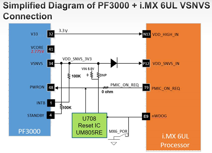
[Answer] “while PWRON pulled up but still we find pulses” seems to be the reason. Is there any reset IC connected to PWRON? This reset IC would better be supplied by VIN 5.0V not directly by VSNVS pin of PF3000.
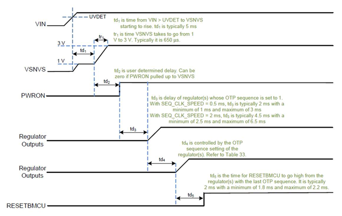
PF3000 PWRON pin should be always high to enable the whole chip and regulators, if PWRON is low, then the PF3000 (all regulators) is in Off mode by default, except any regulators whose SWxOMODE bit is set to “1” during On mode.
See the below connection, please try pull PF3000 PWRON pin always high to enable the whole PMIC, you can see all regulators power up only after PWRON pin is being pulled high. Capturing the PWRON pin waveform is needed for analysis.
Have a great day,
Jose
-----------------------------------------------------------------------------------------------------------------------
Note: If this post answers your question, please click the Correct Answer button. Thank you!
-----------------------------------------------------------------------------------------------------------------------
- 新着としてマーク
- ブックマーク
- 購読
- ミュート
- RSS フィードを購読する
- ハイライト
- 印刷
- 不適切なコンテンツを報告
Hi,
LDOG does not have much configuration, there is only one configurable bit (STBY_LP_B bit) on the Front-end LDO control register (LDOGCTRL), by default, this bit is “0” and when this bit is set to 1, the front-end LDO does not enter in low-power mode during IC standby mode. Which I don’t think it is related to the behavior you are seen.
Can you please confirm if the voltage you are measuring in VIN pin of the PF3000 is 3.4V when the problem is present?
If this is true, then, according to Table 6 of the datasheet, you are seen the VIN at “VIN_OFF” mode which states that the voltage at this pins is in the range of 3.2V and 4.8V.
For the PF3000 the problem with the front-end LDO is often the current consumption in the OFF mode. In the OFF mode we guarantee the Vin (from 3.2 to 4.8 V) only if the current on Vin does not exceed 35µA. This is because the external MOSFET is disabled in OFF mode and a small internal MOSFET is used instead. So, you need to be sure that all the circuitry supplied by Vin do not consume more current (Vin, Vsnvs, ….).
If you sink more current, the Vin drops down and cuts off the regulator then after.
Have a great day,
Jose
-----------------------------------------------------------------------------------------------------------------------
Note: If this post answers your question, please click the Correct Answer button. Thank you!
-----------------------------------------------------------------------------------------------------------------------
- 新着としてマーク
- ブックマーク
- 購読
- ミュート
- RSS フィードを購読する
- ハイライト
- 印刷
- 不適切なコンテンツを報告
Dear Jose Thanks a lot for your reply.
Today we did some work out on our board, which is as below:
- Yesterday as expained we were geting 3.4V at Vin pin (Pin no.42) and LDOG pin 5V (Gate of ext MOSFET) while input was 5V. (You also asked to test this)
- Yesterday we also observed that voltage on PWRNON (pin no. 48) was zero and STANDBY (pin no. 4) was also zero. With this we thought PMIC is in PWROFF or Standby mode.
- Today we connected VDD_SNVS_3V3 supply through 0 Ohm to circuit and PWRON and STANDBY pins got pull up to VDD_SNVS_3V3, which might have brought PMIC out to PWR on mode.
- After above change, we got voltage 4.25V at Vin pin (Pin no.42). This should be atleast 4.3V as per datasheet. However now we moved to test output voltages of PMIC. With this configuration we found all the voltage are coming out from PMIC as expected as per datasheet.
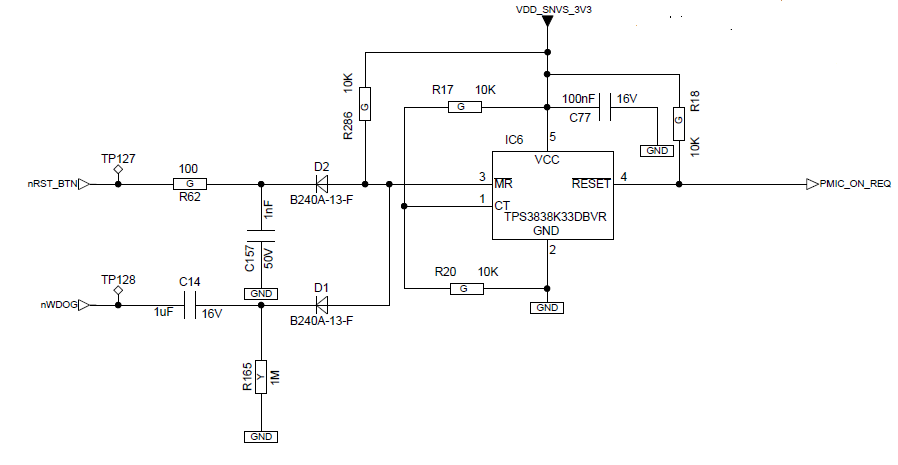
- Now I have certain queries that, I have removed IC6 as shown below circuit, which was loading PMIC_ON_REQ (which is driving PWRON pin of CPU) and keeping the board in PWROFF mode. After removal of tthis chip I got 2.2V pull up on this pin.
- Can I proceed with 4.25V, which is not as per datasheet.
- As you mentioned yesterday that as per Table 6 Ivin should be less than 35uA, but how we can ensure its less than 35uA.
- Can I drive VDD_SNVS_IN rail of CPU by VDD_SNVS_3V3 alone and remaining rails are not driven the CPU. Is it safe to do so?
- I am not sure if I assemble IC6 it will load the PMIC_ON_REQ again and put the board in PWROFF mode.
Waiting for your reply.
Regards,
Surendra
- 新着としてマーク
- ブックマーク
- 購読
- ミュート
- RSS フィードを購読する
- ハイライト
- 印刷
- 不適切なコンテンツを報告
Hi,
I want to add one more thing here that we are independantly testing load capacity of each rail using DC load.
Here we are facing loading issue on SW1A and SW1B. We are trying to draw 100mA of current, but its loading the rails.
Kindly guide us at the earliest.
Regards,
Surendra
- 新着としてマーク
- ブックマーク
- 購読
- ミュート
- RSS フィードを購読する
- ハイライト
- 印刷
- 不適切なコンテンツを報告
Hi,
Input voltage to all regulators is 4.21V as mentioned above is not loading.
However LDOG is varying from 5V to below 5V.
Loading of one rail is impacting other rail outputs also.
Regards,
Surendra
- 新着としてマーク
- ブックマーク
- 購読
- ミュート
- RSS フィードを購読する
- ハイライト
- 印刷
- 不適切なコンテンツを報告
Hi Surendra,
Please check the PF3000 Standby pin (#4 pin) status, it may be high 3.0V thus the PF3000 is in Standby status since by default the PF3000 Standby event triggering is active high of Standby pin.
Two ways:
- Exit Standby status, enter normal On status, then the front-end LDO output ~4.4V will work well.
- If you would like to keep the front-end LDO output normally in Standby status, please set the value of bit STBY_LOWPOWER_B of register 0x69 to “1”, the bit is shown in Table 175 of the datasheet, then it should works as normal On status.
Have a great day,
Jose
-----------------------------------------------------------------------------------------------------------------------
Note: If this post answers your question, please click the Correct Answer button. Thank you!
-----------------------------------------------------------------------------------------------------------------------
- 新着としてマーク
- ブックマーク
- 購読
- ミュート
- RSS フィードを購読する
- ハイライト
- 印刷
- 不適切なコンテンツを報告
Dear Jose,
Thanks a lot for your reply. We had provision to Pull down the Standby pin (#4 pin), which we did and started to get output.
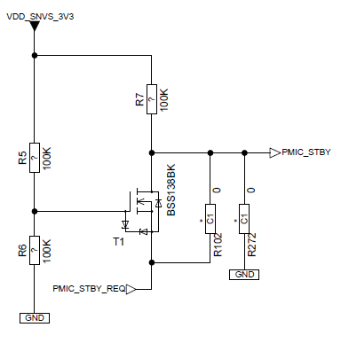
However we have following circuit where we have used following MOSFET based as below.
As for current start, we removed R7 (Pull up and mounted R272) and PMIC is out of standby and we are getting outputs.
Now after assembling CPU and above circuit i.e. removing R272 and mounting R7, will PMIC again enters in Standby mode and no power shall be given to CPU.
- 新着としてマーク
- ブックマーク
- 購読
- ミュート
- RSS フィードを購読する
- ハイライト
- 印刷
- 不適切なコンテンツを報告
Hello,
I have done some testing on above issue. Here I found that I am getting SNVS supply of 3.3V at the output.
Also I could I see PWRON and Standby pins has 0V, which might be putting chip in PWR off or standby mode.
In order to bring PMIC out of this mode, I need pull up on SNVS rail.
I am afraid that if I assembled seies sero ohm resistor and bring the board from PWR off mode to On mode, SNVS voltage will also go to SNVS section of CPU.
Let me know is it safe to give SNVS power to CPU, while other rails are not available.
Regards,
Surendra
- 新着としてマーク
- ブックマーク
- 購読
- ミュート
- RSS フィードを購読する
- ハイライト
- 印刷
- 不適切なコンテンツを報告
Hi,
I am getting 5V at the LDOG pin that is driving gate of MOSFET, while I tested on evaluation board circuit and found that LDOG is 4.012V.
Let me know how one can control this voltage. I suppose this does not need any setting and works by default.
Regards,
Surendra.
