- Forums
- Product Forums
- General Purpose MicrocontrollersGeneral Purpose Microcontrollers
- i.MX Forumsi.MX Forums
- QorIQ Processing PlatformsQorIQ Processing Platforms
- Identification and SecurityIdentification and Security
- Power ManagementPower Management
- Wireless ConnectivityWireless Connectivity
- RFID / NFCRFID / NFC
- Advanced AnalogAdvanced Analog
- MCX Microcontrollers
- S32G
- S32K
- S32V
- MPC5xxx
- Other NXP Products
- S12 / MagniV Microcontrollers
- Powertrain and Electrification Analog Drivers
- Sensors
- Vybrid Processors
- Digital Signal Controllers
- 8-bit Microcontrollers
- ColdFire/68K Microcontrollers and Processors
- PowerQUICC Processors
- OSBDM and TBDML
- S32M
- S32Z/E
-
- Solution Forums
- Software Forums
- MCUXpresso Software and ToolsMCUXpresso Software and Tools
- CodeWarriorCodeWarrior
- MQX Software SolutionsMQX Software Solutions
- Model-Based Design Toolbox (MBDT)Model-Based Design Toolbox (MBDT)
- FreeMASTER
- eIQ Machine Learning Software
- Embedded Software and Tools Clinic
- S32 SDK
- S32 Design Studio
- GUI Guider
- Zephyr Project
- Voice Technology
- Application Software Packs
- Secure Provisioning SDK (SPSDK)
- Processor Expert Software
- Generative AI & LLMs
-
- Topics
- Mobile Robotics - Drones and RoversMobile Robotics - Drones and Rovers
- NXP Training ContentNXP Training Content
- University ProgramsUniversity Programs
- Rapid IoT
- NXP Designs
- SafeAssure-Community
- OSS Security & Maintenance
- Using Our Community
-
- Cloud Lab Forums
-
- Knowledge Bases
- ARM Microcontrollers
- i.MX Processors
- Identification and Security
- Model-Based Design Toolbox (MBDT)
- QorIQ Processing Platforms
- S32 Automotive Processing Platform
- Wireless Connectivity
- CodeWarrior
- MCUXpresso Suite of Software and Tools
- MQX Software Solutions
- RFID / NFC
- Advanced Analog
-
- NXP Tech Blogs
- Home
- :
- i.MX Forums
- :
- i.MX Processors
- :
- Re: Need support for SAI_RX2 issue
Need support for SAI_RX2 issue
- Subscribe to RSS Feed
- Mark Topic as New
- Mark Topic as Read
- Float this Topic for Current User
- Bookmark
- Subscribe
- Mute
- Printer Friendly Page
Need support for SAI_RX2 issue
- Mark as New
- Bookmark
- Subscribe
- Mute
- Subscribe to RSS Feed
- Permalink
- Report Inappropriate Content
Hi NXP support,
IMX is the master, and the tuner is slave.
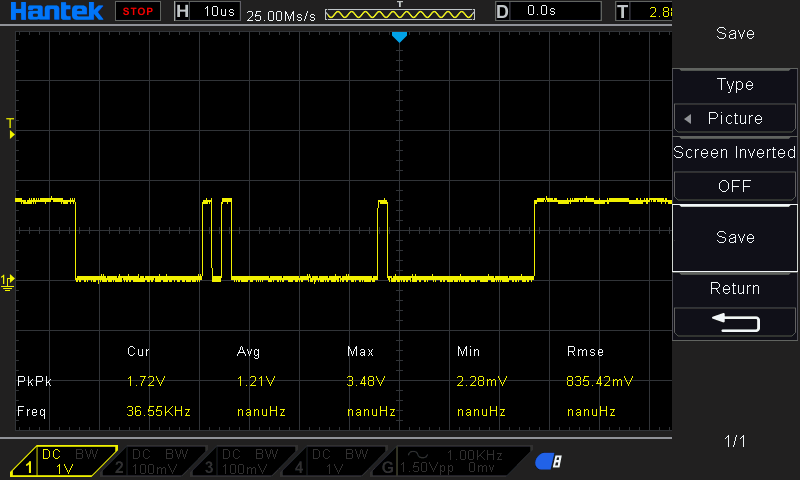
If we monitor the connection, we can see that the signal is squeeze to 0 and almost 0V (see attached picture)
We have done the test of connecting the tuner to SAI1_RX0 (instead of SAI1_RX2) and it we did get the correct signal/data.
That means the issue is on the IMX side, we think this can be a pin config issue as the DISP_B2_01 is SAI1_RX2 and SAI1_TX2 but we don't know how to force RX mode.
Here some SAI1 registry dump during transfers
tcr1: 0x10 tcr2: 0x7000007 tcr3: 0x10000 tcr4: 0x10010f3b tcr5: 0xf0f0f00
rcr1: 0x10 rcr2: 0x47000007 rcr3: 0x40000 rcr4: 0x10010f1b rcr5: 0xf0f0f00
- Mark as New
- Bookmark
- Subscribe
- Mute
- Subscribe to RSS Feed
- Permalink
- Report Inappropriate Content
Thanks so much for @Aubineau_FAE and @eric_delanghe 's effort!
Setting TCR4[5]=0 (CHMOD) will affect SAI1.TX_DATA[0] function in some applications, for example as follow:
SAI1 data line can be configured to Stereo mode, MonoRight mode, MonoLeft mode.
If SAI1.TX_DATA[0] is configured to MonoLeft mode(right channel masked), and SAI1.RX_DATA[1] can receive PCM data(TCR4[5] =0), the right channel data state is determined by the last valid bit of left channel data.
So, I suggest you don't use the TX as MonoLeft mode, just to avoid the limit with CHMOD=0.
If you have any more detail issues, welcome to create the new question post. If this quesiton is solved, please help to mark the correct answer, just to close this case.
Wish it helps you!
Best Regards,
Kerry
- Mark as New
- Bookmark
- Subscribe
- Mute
- Subscribe to RSS Feed
- Permalink
- Report Inappropriate Content
Hi @LydieCDO ,
Please also try to modify your pinmux like this:
IOMUXC_SetPinMux(
      IOMUXC_GPIO_DISP_B2_00_SAI1_TX_DATA03,  /* GPIO_DISP_B2_00 is configured as SAI1_TX_DATA03 */
      1U);                                    /* Software Input On Field: Input Path is determined by functionality */
  IOMUXC_SetPinMux(
      IOMUXC_GPIO_DISP_B2_01_SAI1_TX_DATA02,  /* GPIO_DISP_B2_01 is configured as SAI1_TX_DATA02 */
      1U);                                    /* Software Input On Field: Input Path is determined by functionality */
  IOMUXC_SetPinMux(
      IOMUXC_GPIO_DISP_B2_02_SAI1_TX_DATA01,  /* GPIO_DISP_B2_02 is configured as SAI1_TX_DATA01 */
      1U);                                    /* Software Input On Field: Input Path is determined by functionality */
  IOMUXC_SetPinMux(
      IOMUXC_GPIO_DISP_B2_03_SAI1_MCLK,       /* GPIO_DISP_B2_03 is configured as SAI1_MCLK */
      1U);                                    /* Software Input On Field: Input Path is determined by functionality */

  IOMUXC_SetPinMux(
      IOMUXC_GPIO_DISP_B2_06_SAI1_RX_DATA00,  /* GPIO_DISP_B2_06 is configured as SAI1_RX_DATA00 */
      1U);                                    /* Software Input On Field: Input Path is determined by functionality */
  IOMUXC_SetPinMux(
      IOMUXC_GPIO_DISP_B2_07_SAI1_TX_DATA00,  /* GPIO_DISP_B2_07 is configured as SAI1_TX_DATA00 */
      1U);                                    /* Software Input On Field: Input Path is determined by functionality */
  IOMUXC_SetPinMux(
      IOMUXC_GPIO_DISP_B2_08_SAI1_TX_BCLK,    /* GPIO_DISP_B2_08 is configured as SAI1_TX_BCLK */
      1U);                                    /* Software Input On Field: Input Path is determined by functionality */
  IOMUXC_SetPinMux(
      IOMUXC_GPIO_DISP_B2_09_SAI1_TX_SYNC,    /* GPIO_DISP_B2_09 is configured as SAI1_TX_SYNC */
      1U);                                    /* Software Input On Field: Input Path is determined by functionality */
Our SDK SAI code also set the software input on field as 1, you can try it on your side, whether your SAI receive still have issues or not.
Any updated information, just kindly let us know.
Best Regards,
Kerry
- Mark as New
- Bookmark
- Subscribe
- Mute
- Subscribe to RSS Feed
- Permalink
- Report Inappropriate Content
Hello,
I just tried with a pinmux configured like this and nothing changed.
Do you know if there is anything to do on the SAI registers ?
Best regards,
Eric
- Mark as New
- Bookmark
- Subscribe
- Mute
- Subscribe to RSS Feed
- Permalink
- Report Inappropriate Content
Hi @eric_delanghe ,
Thanks for your effort.
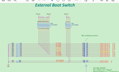
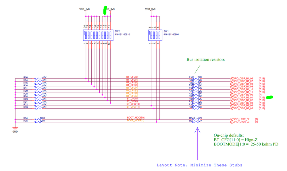
GPIO_DISP_B2_01 is also the BT_CFG[7], and in the MIMXRT1170-EVK board, it connect to the ground through the 47K resistor:
If no external input, it will be 0 in default.
Can you please test it like this:
I. disconnect your external wave to connect the board,
2 reset or POR,
3. after it boot, then connect your external SAI1_RXD[2], and check the wave, whether your external SAI can input the data to the RXD[2]?
If you still have issues, can you reproduce the issues on the NXP MIMXRT1170-EVK board, then I can help you to test it on my side.
Best Regards,
Kerry
- Mark as New
- Bookmark
- Subscribe
- Mute
- Subscribe to RSS Feed
- Permalink
- Report Inappropriate Content
Hello,
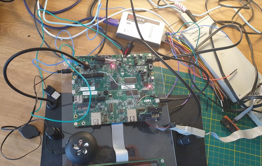
I successfully reproduced on EVK
I removed the jumper on J61 and connected a wire from the MCU side of R775 (SAI1_RXD[2]) to J61 on codec side (SAI1_RXD[0])
It mean that ADCDAT of WM8960 is connected to GPIO_DISP_B2_01.
I use the demo code from SDK "boards/evkmimxrt1170/demo_apps/sai/cm7" and do the following change
diff --git a/boards/evkmimxrt1170/demo_apps/sai/cm7/board.h b/boards/evkmimxrt1170/demo_apps/sai/cm7/board.h
index 790dbf5e..d8816bdf 100644
--- a/boards/evkmimxrt1170/demo_apps/sai/cm7/board.h
+++ b/boards/evkmimxrt1170/demo_apps/sai/cm7/board.h
@@ -122,7 +122,7 @@
 #define BOARD_ARDUINO_I2C_IRQ   (LPI2C1_IRQn)
 #define BOARD_ARDUINO_I2C_INDEX (1)

-#define BOARD_HAS_SDCARD (1U)
+#define BOARD_HAS_SDCARD (0U)

 /* @Brief Board accelerator sensor configuration */
 #define BOARD_ACCEL_I2C_BASEADDR LPI2C5
diff --git a/boards/evkmimxrt1170/demo_apps/sai/cm7/pin_mux.c b/boards/evkmimxrt1170/demo_apps/sai/cm7/pin_mux.c
index 32343576..d4941b89 100644
--- a/boards/evkmimxrt1170/demo_apps/sai/cm7/pin_mux.c
+++ b/boards/evkmimxrt1170/demo_apps/sai/cm7/pin_mux.c
@@ -79,6 +79,9 @@ void BOARD_InitPins(void) {
   IOMUXC_SetPinMux(
       IOMUXC_GPIO_AD_20_SAI1_RX_DATA00,       /* GPIO_AD_20 is configured as SAI1_RX_DATA00 */
       1U);                                    /* Software Input On Field: Force input path of pad GPIO_AD_20 */
+  IOMUXC_SetPinMux(
+      IOMUXC_GPIO_DISP_B2_01_SAI1_TX_DATA02,  /* GPIO_DISP_B2_01 is configured as SAI1_TX_DATA02 */
+      1U);                                    /* Software Input On Field: Input Path is determined by functionality */
   IOMUXC_SetPinMux(
       IOMUXC_GPIO_AD_21_SAI1_TX_DATA00,       /* GPIO_AD_21 is configured as SAI1_TX_DATA00 */
       1U);                                    /* Software Input On Field: Force input path of pad GPIO_AD_21 */
diff --git a/boards/evkmimxrt1170/demo_apps/sai/cm7/sai.c b/boards/evkmimxrt1170/demo_apps/sai/cm7/sai.c
index 1a62ffb1..470f3e7c 100644
--- a/boards/evkmimxrt1170/demo_apps/sai/cm7/sai.c
+++ b/boards/evkmimxrt1170/demo_apps/sai/cm7/sai.c
@@ -331,11 +331,13 @@ int main(void)
     SAI_TransferRxCreateHandleEDMA(DEMO_SAI, &rxHandle, rxCallback, NULL, &dmaRxHandle);

     /* I2S mode configurations */
-    SAI_GetClassicI2SConfig(&saiConfig, DEMO_AUDIO_BIT_WIDTH, kSAI_Stereo, 1U << DEMO_SAI_CHANNEL);
+    SAI_GetClassicI2SConfig(&saiConfig, DEMO_AUDIO_BIT_WIDTH, kSAI_Stereo, 0x7);
     saiConfig.syncMode    = DEMO_SAI_TX_SYNC_MODE;
     saiConfig.masterSlave = DEMO_SAI_MASTER_SLAVE;
+    saiConfig.channelMask = kSAI_Channel0Mask;
     SAI_TransferTxSetConfigEDMA(DEMO_SAI, &txHandle, &saiConfig);
     saiConfig.syncMode = DEMO_SAI_RX_SYNC_MODE;
+    saiConfig.channelMask = kSAI_Channel2Mask;
     SAI_TransferRxSetConfigEDMA(DEMO_SAI, &rxHandle, &saiConfig);

     /* set bit clock divider */
If I look with the oscilloscope, I get the same result, data is 0.3V when high
- Mark as New
- Bookmark
- Subscribe
- Mute
- Subscribe to RSS Feed
- Permalink
- Report Inappropriate Content
Hi,
I confirm your code does not work on the EVK ("1. Record and playback at same time" used).
Instead please do the following init sequence:
/* I2S mode configurations */
//SAI_GetClassicI2SConfig(&saiConfig, DEMO_AUDIO_BIT_WIDTH, kSAI_Stereo, 7);
SAI_GetClassicI2SConfig(&saiConfig, DEMO_AUDIO_BIT_WIDTH, kSAI_Stereo, kSAI_Channel0Mask);
saiConfig.syncMode = DEMO_SAI_TX_SYNC_MODE;
saiConfig.masterSlave = DEMO_SAI_MASTER_SLAVE;
saiConfig.channelMask = kSAI_Channel0Mask;
SAI_TransferTxSetConfigEDMA(DEMO_SAI, &txHandle, &saiConfig);
SAI_GetClassicI2SConfig(&saiConfig, DEMO_AUDIO_BIT_WIDTH, kSAI_Stereo, kSAI_Channel2Mask|kSAI_Channel1Mask);
saiConfig.masterSlave = DEMO_SAI_MASTER_SLAVE;
saiConfig.syncMode = DEMO_SAI_RX_SYNC_MODE;
saiConfig.channelMask = kSAI_Channel2Mask;
SAI_TransferRxSetConfigEDMA(DEMO_SAI, &rxHandle, &saiConfig);
GPIO_DISP_B2_01 (R775) is toggling and I can hear noise in my loudspeaker:
- Channel 0 -> SAI1_TX[0] (J9 pin 9)
- Channel 1 -> SAI1_RX[2] (R775)
/Vincent
- Mark as New
- Bookmark
- Subscribe
- Mute
- Subscribe to RSS Feed
- Permalink
- Report Inappropriate Content
Hello Vincent
I've took your init sequence but still not able to see or heard anything.
Can you send me your binary, so I can try it here ?
Best regards,
Eric
- Mark as New
- Bookmark
- Subscribe
- Mute
- Subscribe to RSS Feed
- Permalink
- Report Inappropriate Content
- Mark as New
- Bookmark
- Subscribe
- Mute
- Subscribe to RSS Feed
- Permalink
- Report Inappropriate Content
Hi,
I did measure with an oscilloscope instead of a logic analyzer.
Actually the voltage level is #1.6V / #1.3V depending of the DSE.
I have the same behavior if I configure the pin as GPIO11_IO2 in output mode (so not 3V3):
We'll get back to you asap.
Vincent
- Mark as New
- Bookmark
- Subscribe
- Mute
- Subscribe to RSS Feed
- Permalink
- Report Inappropriate Content
Hi,
InTCR4, CHMOD bitfield to 0:
On my side I got full range then (3V3).
Vincent
- Mark as New
- Bookmark
- Subscribe
- Mute
- Subscribe to RSS Feed
- Permalink
- Report Inappropriate Content
Hello Vincent,
Yes it work ! I finally can heard FM coming from the Tuner
Thanks a lot for your investigation !
Best regards,
Delanghe Eric
- Mark as New
- Bookmark
- Subscribe
- Mute
- Subscribe to RSS Feed
- Permalink
- Report Inappropriate Content
Hi,
What do you mean by "external wave" ?
Are you talking about the data lane (DOUT0) from the tuner ?
best regards,
Eric
- Mark as New
- Bookmark
- Subscribe
- Mute
- Subscribe to RSS Feed
- Permalink
- Report Inappropriate Content
- Mark as New
- Bookmark
- Subscribe
- Mute
- Subscribe to RSS Feed
- Permalink
- Report Inappropriate Content
Thanks for taking this issue
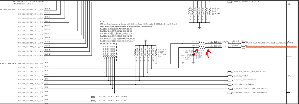
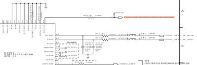
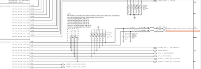
Here the schematic:
Tuner side:
  IOMUXC_SetPinMux(
      IOMUXC_GPIO_DISP_B2_00_SAI1_TX_DATA03,  /* GPIO_DISP_B2_00 is configured as SAI1_TX_DATA03 */
      0U);                                    /* Software Input On Field: Input Path is determined by functionality */
  IOMUXC_SetPinMux(
      IOMUXC_GPIO_DISP_B2_01_SAI1_TX_DATA02,  /* GPIO_DISP_B2_01 is configured as SAI1_TX_DATA02 */
      0U);                                    /* Software Input On Field: Input Path is determined by functionality */
  IOMUXC_SetPinMux(
      IOMUXC_GPIO_DISP_B2_02_SAI1_TX_DATA01,  /* GPIO_DISP_B2_02 is configured as SAI1_TX_DATA01 */
      0U);                                    /* Software Input On Field: Input Path is determined by functionality */
  IOMUXC_SetPinMux(
      IOMUXC_GPIO_DISP_B2_03_SAI1_MCLK,       /* GPIO_DISP_B2_03 is configured as SAI1_MCLK */
      0U);                                    /* Software Input On Field: Input Path is determined by functionality */

  IOMUXC_SetPinMux(
      IOMUXC_GPIO_DISP_B2_06_SAI1_RX_DATA00,  /* GPIO_DISP_B2_06 is configured as SAI1_RX_DATA00 */
      0U);                                    /* Software Input On Field: Input Path is determined by functionality */
  IOMUXC_SetPinMux(
      IOMUXC_GPIO_DISP_B2_07_SAI1_TX_DATA00,  /* GPIO_DISP_B2_07 is configured as SAI1_TX_DATA00 */
      0U);                                    /* Software Input On Field: Input Path is determined by functionality */
  IOMUXC_SetPinMux(
      IOMUXC_GPIO_DISP_B2_08_SAI1_TX_BCLK,    /* GPIO_DISP_B2_08 is configured as SAI1_TX_BCLK */
      0U);                                    /* Software Input On Field: Input Path is determined by functionality */
  IOMUXC_SetPinMux(
      IOMUXC_GPIO_DISP_B2_09_SAI1_TX_SYNC,    /* GPIO_DISP_B2_09 is configured as SAI1_TX_SYNC */
      0U);                                    /* Software Input On Field: Input Path is determined by functionality */
     SAI_GetClassicI2SConfig(&priv->I2SConfig, bit_width, is_stereo, priv->sai_chan);

    priv->I2SConfig.masterSlave = kSAI_Master;
    /* Note: See 58.3.2.1 Synchronous mode */
    priv->I2SConfig.channelMask = kSAI_Channel0Mask;
    priv->I2SConfig.syncMode = kSAI_ModeAsync;
    SAI_TransferTxSetConfigEDMA(priv->sai, &(priv->txHandle), &priv->I2SConfig);
    priv->oneTxFrame = priv->txHandle.count * priv->txHandle.bytesPerFrame;

    priv->I2SConfig.channelMask = kSAI_Channel2Mask;
    priv->I2SConfig.syncMode = kSAI_ModeSync;
    SAI_TransferRxSetConfigEDMA(priv->sai, &(priv->rxHandle), &priv->I2SConfig);
    priv->oneRxFrame = priv->rxHandle.count * priv->rxHandle.bytesPerFrame;

    /* set bit clock divider */
    /* Divide Root_SAIX clock (mclk) to bclk */
    SAI_TxSetBitClockRate(priv->sai, clock_rate, sampling_rate, bit_width, nb_channel);
    SAI_RxSetBitClockRate(priv->sai, clock_rate, sampling_rate, bit_width, nb_channel);
Thanks again
- Mark as New
- Bookmark
- Subscribe
- Mute
- Subscribe to RSS Feed
- Permalink
- Report Inappropriate Content
I've checked configuration with Reference Manual and Pin tool and everything looks correct. Output from tuner has 3-state, Hi-Z, is there any internal pull-up inside tuner? it looks that there is greater pull-down what I see from oscilloscope image.
Mike
- Mark as New
- Bookmark
- Subscribe
- Mute
- Subscribe to RSS Feed
- Permalink
- Report Inappropriate Content
Hello @mike_susen
I'll ask tuner team for this but I'm not sure if this is related because if we connect the DOUT0(tuner) on SAI1_RX0(imx) the transfer work correctly.
Best regards,
Eric
- Mark as New
- Bookmark
- Subscribe
- Mute
- Subscribe to RSS Feed
- Permalink
- Report Inappropriate Content
are you sure that you not accessing the GPIO registers on this pin? It is not possible to have hard pull-down in this case.
Edit: DISP_B2_01 has internal PD turned on instedad of DISP_B2_06 which has HighZ mode. try to tune SW_PAD_CTL_PAD_GPIO_DISP_B2_01 SW PAD Control
Register (SW_PAD_CTL_PAD_GPIO_DISP_B2_01) to disable PD or switch to HighZ.
Mike
- Mark as New
- Bookmark
- Subscribe
- Mute
- Subscribe to RSS Feed
- Permalink
- Report Inappropriate Content
Hello @mike_susen ,
Thanks for your support
Also sorry for this late answer, I was busy on something else.
I've done the test and nothing changed.
I use NXP Config tool to generate the following line
  IOMUXC_SetPinConfig(
      IOMUXC_GPIO_DISP_B2_01_SAI1_TX_DATA02,  /* GPIO_DISP_B2_01 PAD functional properties : */
      0x02U);                                 /* Slew Rate Field: Slow Slew Rate
                                                 Drive Strength Field: high drive strength
                                                 Pull / Keep Select Field: Pull Disable, Highz
                                                 Pull Up / Down Config. Field: Weak pull down
                                                 Open Drain Field: Disabled
                                                 Domain write protection: Both cores are allowed
                                                 Domain write protection lock: Neither of DWP bits is locked */
I tried with the following values
| 0x0 | default |
| 0x2 | high drive strength |
| 0x4 | HIGHZ |
| 0x6 | HIGHZ, high drive strength |
But it never worked.
Any other idea ?
Best regards,
Eric
- Mark as New
- Bookmark
- Subscribe
- Mute
- Subscribe to RSS Feed
- Permalink
- Report Inappropriate Content
Hi,
Can you confirm you see the signal disappearing if you do the measures on the 2 sides of the resistor, see below:
I have modified the SDK code and configured the pin as below:
 IOMUXC_SetPinMux(
IOMUXC_GPIO_DISP_B2_01_SAI1_TX_DATA02, /* GPIO_DISP_B2_01 is configured as SAI1_TX_DATA02 */
0U); /* Software Input On Field: Input Path is determined by functionality */
IOMUXC_SetPinMux(
IOMUXC_GPIO_DISP_B2_00_SAI1_TX_DATA03, /* GPIO_DISP_B2_00 is configured as SAI1_TX_DATA03 */
0U); /* Software Input On Field: Input Path is determined by functionality */
and measured the voltage on the switch:
And I see (logic analyser) no contention if I toggle the switch.
Did you check the IOMUX register is configured as expected with a JTAG probe?
Vincent
- Mark as New
- Bookmark
- Subscribe
- Mute
- Subscribe to RSS Feed
- Permalink
- Report Inappropriate Content
Hello,
I just tried and get the same result on both side of R4261
Also I use gdb to check and registers are right.
Best regards,
Eric
