- Forums
- Product Forums
- General Purpose MicrocontrollersGeneral Purpose Microcontrollers
- i.MX Forumsi.MX Forums
- QorIQ Processing PlatformsQorIQ Processing Platforms
- Identification and SecurityIdentification and Security
- Power ManagementPower Management
- Wireless ConnectivityWireless Connectivity
- RFID / NFCRFID / NFC
- MCX Microcontrollers
- S32G
- S32K
- S32V
- MPC5xxx
- Other NXP Products
- S12 / MagniV Microcontrollers
- Powertrain and Electrification Analog Drivers
- Sensors
- Vybrid Processors
- Digital Signal Controllers
- 8-bit Microcontrollers
- ColdFire/68K Microcontrollers and Processors
- PowerQUICC Processors
- OSBDM and TBDML
- S32M
-
- Solution Forums
- Software Forums
- MCUXpresso Software and ToolsMCUXpresso Software and Tools
- CodeWarriorCodeWarrior
- MQX Software SolutionsMQX Software Solutions
- Model-Based Design Toolbox (MBDT)Model-Based Design Toolbox (MBDT)
- FreeMASTER
- eIQ Machine Learning Software
- Embedded Software and Tools Clinic
- S32 SDK
- S32 Design Studio
- GUI Guider
- Zephyr Project
- Voice Technology
- Application Software Packs
- Secure Provisioning SDK (SPSDK)
- Processor Expert Software
-
- Topics
- Mobile Robotics - Drones and RoversMobile Robotics - Drones and Rovers
- NXP Training ContentNXP Training Content
- University ProgramsUniversity Programs
- Rapid IoT
- NXP Designs
- SafeAssure-Community
- OSS Security & Maintenance
- Using Our Community
-
- Cloud Lab Forums
-
- Knowledge Bases
- ARM Microcontrollers
- i.MX Processors
- Identification and Security
- Model-Based Design Toolbox (MBDT)
- QorIQ Processing Platforms
- S32 Automotive Processing Platform
- Wireless Connectivity
- CodeWarrior
- MCUXpresso Suite of Software and Tools
- MQX Software Solutions
-
GPIO_EMC_39
Hello,
We are using the MIMXRT1051CVL5B in our design.
We are encountering an issue with the B7 pin (GPIO_EMC_39).
We have configured this signal as an input, but when we press the POR button, this pin is driving our external circuit low (we have connected a '1' push-pull configuration to that pin).
Could you please assist us in understanding why this issue is occurring and how we can prevent the MCU from driving it low?
Hi @sapirbuz,
As mentioned on the RM, on section "11.6.164 SW_PAD_CTL_PAD_GPIO_EMC_39 SW PAD Control Register (IOMUXC_SW_PAD_CTL_PAD_GPIO_EMC_39)" bit field "Pull Up / Down Config. Field" is initialized to a "00 PUS_0_100K_Ohm_Pull_Down — 100K Ohm Pull Down" after reset. This is why you are seeing the pin low after a POR.
BR,
Edwin.
Hi,
IOMUXC_SW_PAD_CTL_PAD_GPIO_EMC_41 is defined the same as IOMUXC_SW_PAD_CTL_PAD_GPIO_EMC_39, but it isn't driven low while POR.
How can we prevent IOMUXC_SW_PAD_CTL_PAD_GPIO_EMC_39 from driving our signal to low after POR?
Hi @sapirbuz,
Are you currently using the Device Configuration Data (DCD) to set up GPIO_EMC_39? i.e.:
 /* #1.90, command: write_value, address: IOMUXC_SW_PAD_CTL_PAD_GPIO_EMC_39, value: 0x110F9, size: 4 */
0x40, 0x1F, 0x82, 0xA0, 0x00, 0x01, 0x10, 0xF9,
BR,
Edwin.
Hi @sapirbuz,
This is most likely why this specific pin is being changed upon boot. If you don't use this pin to operate an external memory upon boot, then you should be able to remove it, and the pin will not be configured upon boot.
BR,
Edwin.
Hi,
we removed the following:
/* #1.90, command: write_value, address: IOMUXC_SW_PAD_CTL_PAD_GPIO_EMC_39, value: 0x110F9, size: 4 */
0x40, 0x1F, 0x82, 0xA0, 0x00, 0x01, 0x10, 0xF9,
and the issue wasn't solved
Hi @sapirbuz,
Could you please share the external circuit that you are connecting to the pad? Perhaps the issue lies in the hardware configuration of the pin, rather than the software configuration.
BR,
Edwin.
Hi @sapirbuz,
This issue is most likely caused by conflicts of the DQS functionality of this pad. Could you please share if you are using SEMC functionality to handle an external memory? What type of memory would that be? Also, please check the GPIO/fuse BOOT_CFG [10] (depending on if there is GPIO override or not). Is the "DQS pin pad enablement" on 1 or 0?
Hi,
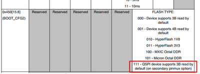
SEMC is used, and the external memory is NOR secondary, as in Picture 1.
BOOT_CFG[10] is configured as input GPIO, PU and keeper are defined as no init.
the DQS pins were left unconnected by HW.
At the beginning, DQS pins were enabled, but the MCU couldn't read the data from the boot EEPROM; so we disabled those pins.
Picture 1:
Hi @sapirbuz,
I am still looking into this issue. Could you please double check that the BOOT_CFG[10] fuse is still on 0 (unburned)?
It could be an issue that, during booting, the fuse selection of this pin is affecting its functionality, so we need to make sure the DQS fuse is not enabled on fuses for this pad.

