- Forums
- Product Forums
- General Purpose MicrocontrollersGeneral Purpose Microcontrollers
- i.MX Forumsi.MX Forums
- QorIQ Processing PlatformsQorIQ Processing Platforms
- Identification and SecurityIdentification and Security
- Power ManagementPower Management
- Wireless ConnectivityWireless Connectivity
- RFID / NFCRFID / NFC
- MCX Microcontrollers
- S32G
- S32K
- S32V
- MPC5xxx
- Other NXP Products
- S12 / MagniV Microcontrollers
- Powertrain and Electrification Analog Drivers
- Sensors
- Vybrid Processors
- Digital Signal Controllers
- 8-bit Microcontrollers
- ColdFire/68K Microcontrollers and Processors
- PowerQUICC Processors
- OSBDM and TBDML
- S32M
-
- Solution Forums
- Software Forums
- MCUXpresso Software and ToolsMCUXpresso Software and Tools
- CodeWarriorCodeWarrior
- MQX Software SolutionsMQX Software Solutions
- Model-Based Design Toolbox (MBDT)Model-Based Design Toolbox (MBDT)
- FreeMASTER
- eIQ Machine Learning Software
- Embedded Software and Tools Clinic
- S32 SDK
- S32 Design Studio
- GUI Guider
- Zephyr Project
- Voice Technology
- Application Software Packs
- Secure Provisioning SDK (SPSDK)
- Processor Expert Software
-
- Topics
- Mobile Robotics - Drones and RoversMobile Robotics - Drones and Rovers
- NXP Training ContentNXP Training Content
- University ProgramsUniversity Programs
- Rapid IoT
- NXP Designs
- SafeAssure-Community
- OSS Security & Maintenance
- Using Our Community
-
- Cloud Lab Forums
-
- Knowledge Bases
- ARM Microcontrollers
- i.MX Processors
- Identification and Security
- Model-Based Design Toolbox (MBDT)
- QorIQ Processing Platforms
- S32 Automotive Processing Platform
- Wireless Connectivity
- CodeWarrior
- MCUXpresso Suite of Software and Tools
- MQX Software Solutions
-
- Home
- :
- i.MX Forums
- :
- i.MX Processors
- :
- DDR Stress Test failed for IMX8QM Custom Board
DDR Stress Test failed for IMX8QM Custom Board
- Subscribe to RSS Feed
- Mark Topic as New
- Mark Topic as Read
- Float this Topic for Current User
- Bookmark
- Subscribe
- Mute
- Printer Friendly Page
- Mark as New
- Bookmark
- Subscribe
- Mute
- Subscribe to RSS Feed
- Permalink
- Report Inappropriate Content
Dear NXP,
DDR stress test failed. Will you please give some idea regarding the following errors,
*************************************************************************
MX8 DDR Stress Test Version: ER14
Built on Mar 27 2020 12:19:30
*************************************************************************
--Set up the MMU and enable I and D cache--
- This is the Cortex-A72 core
Adjusting CA72 cache latency
- Check if I cache is enabled
- Enabling I cache since it was disabled
- Push base address of TTB to TTBR0_EL3
- Config TCR_EL3
- Config MAIR_EL3
- Enable MMU
- Data Cache has been enabled
- Check system memory register, only for debug
- VMCR Check:
- ttbr0_el3: 0x13d000
- tcr_el3: 0x2051c
- mair_el3: 0x774400
- sctlr_el3: 0xc01815
- id_aa64mmfr0_el1: 0x1124
- MMU and cache setup complete
*************************************************************************
ARM Clock(CA72): 1596MHz
DDR Clock: 1596MHz
============================================
DDR configuration
DDR type is LPDDR4
Data width: 32, bank num: 8
Row size: 15, col size: 10
Two chip selects are used
Number of DDR controllers used on the SoC: 2
Density per chip select: 1024MB
Density per controller is: 2048MB
Total density detected on the board is: 4096MB
Note: As this SoC has more than one DDR Controller, the calculated
density assumes all controllers are being used. Adjust the tested
density per your board configuration if not all controllers are used
********************************************
WARNING! DDR training errors were detected on DDRC 0!
DDR_PHY_PGSR0 = 0x806cc07f
DQS Gate training error detected
Write Leveling training error detected
VREF training error detected
Write DQS2DQ training error detected
Recheck DDR initialization
********************************************
********************************************
WARNING! DDR training errors were detected on DDRC 1!
DDR_PHY_PGSR0 = 0x806cc07f
DQS Gate training error detected
Write Leveling training error detected
VREF training error detected
Write DQS2DQ training error detected
Recheck DDR initialization
********************************************
============================================
MX8QM: Cortex-A72 is found
*************************************************************************
Vinothkumar Sekar
Solved! Go to Solution.
- Mark as New
- Bookmark
- Subscribe
- Mute
- Subscribe to RSS Feed
- Permalink
- Report Inappropriate Content
I believe Chan B is configured incorrectly. For example:
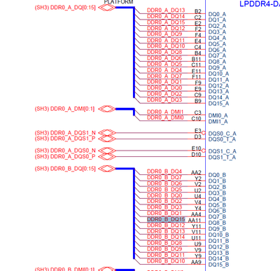
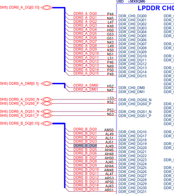
on your schematic DQ0_B (pad AA2) is connected to DDR0_B_DQ4 (DDR_CH0_DQ20)
so Excel "BoardDataBusConfig" Chan B should be:
DRAM Data bus 0
MX8QM data bus (User Input)-> 20
DQ1_B (pad Y2) is connected to DDR0_B_DQ7 (DDR_CH0_DQ23)
so Excel "BoardDataBusConfig" should be:
DRAM Data bus 1
MX8QM data bus (User Input)-> 23
e.t.c.
Best regards
igor
- Mark as New
- Bookmark
- Subscribe
- Mute
- Subscribe to RSS Feed
- Permalink
- Report Inappropriate Content
Hi Vinothkumar
reason for this issue may be wrong memory connections or incorrectly configured "BoardDataBusConfig"
parameters in RPA tool.
Best regards
igor
- Mark as New
- Bookmark
- Subscribe
- Mute
- Subscribe to RSS Feed
- Permalink
- Report Inappropriate Content
Thank you @igorpadykov for the reply.
Will you please validate my BoardDataBusConfig section for DDRC0.
Vinothkumar Sekar
- Mark as New
- Bookmark
- Subscribe
- Mute
- Subscribe to RSS Feed
- Permalink
- Report Inappropriate Content
I believe Chan B is configured incorrectly. For example:
on your schematic DQ0_B (pad AA2) is connected to DDR0_B_DQ4 (DDR_CH0_DQ20)
so Excel "BoardDataBusConfig" Chan B should be:
DRAM Data bus 0
MX8QM data bus (User Input)-> 20
DQ1_B (pad Y2) is connected to DDR0_B_DQ7 (DDR_CH0_DQ23)
so Excel "BoardDataBusConfig" should be:
DRAM Data bus 1
MX8QM data bus (User Input)-> 23
e.t.c.
Best regards
igor

