- Forums
- Product Forums
- General Purpose MicrocontrollersGeneral Purpose Microcontrollers
- i.MX Forumsi.MX Forums
- QorIQ Processing PlatformsQorIQ Processing Platforms
- Identification and SecurityIdentification and Security
- Power ManagementPower Management
- MCX Microcontrollers
- S32G
- S32K
- S32V
- MPC5xxx
- Other NXP Products
- Wireless Connectivity
- S12 / MagniV Microcontrollers
- Powertrain and Electrification Analog Drivers
- Sensors
- Vybrid Processors
- Digital Signal Controllers
- 8-bit Microcontrollers
- ColdFire/68K Microcontrollers and Processors
- PowerQUICC Processors
- OSBDM and TBDML
- S32M
-
- Solution Forums
- Software Forums
- MCUXpresso Software and ToolsMCUXpresso Software and Tools
- CodeWarriorCodeWarrior
- MQX Software SolutionsMQX Software Solutions
- Model-Based Design Toolbox (MBDT)Model-Based Design Toolbox (MBDT)
- FreeMASTER
- eIQ Machine Learning Software
- Embedded Software and Tools Clinic
- S32 SDK
- S32 Design Studio
- GUI Guider
- Zephyr Project
- Voice Technology
- Application Software Packs
- Secure Provisioning SDK (SPSDK)
- Processor Expert Software
- MCUXpresso Training Hub
-
- Topics
- Mobile Robotics - Drones and RoversMobile Robotics - Drones and Rovers
- NXP Training ContentNXP Training Content
- University ProgramsUniversity Programs
- Rapid IoT
- NXP Designs
- SafeAssure-Community
- OSS Security & Maintenance
- Using Our Community
-
- Cloud Lab Forums
-
- Knowledge Bases
- ARM Microcontrollers
- i.MX Processors
- Identification and Security
- Model-Based Design Toolbox (MBDT)
- QorIQ Processing Platforms
- S32 Automotive Processing Platform
- Wireless Connectivity
- CodeWarrior
- MCUXpresso Suite of Software and Tools
- MQX Software Solutions
-
We need some advice about Power block of i.MX28.
We are planning to use DCDC_BATT source only configuration and to make it cheap, the supply voltage be 3.3V for normal operation.
However, since we are also planning to download firmware to NAND flash via MfgTool, the configuration will be 5V source only during download process.
The question is, how do you apply bias to DCDC_BATT and BATTERY during download process if you use the circuit shown in Figure 8 of AN4199?
Will adding another diode next to D1 which is facing the opposite direction work?
Can anyone give us some advice about how to design the Power block?
Or could anyone who made similar board show us the Power block of your schematics, please? We really appreciate it.
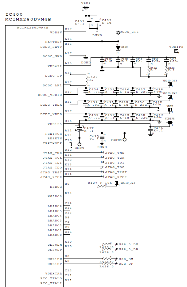
The schematic below is our draft.
As you can guess, DCDC_3P3 is derived from a dcdc converter and VBUS is connected to USB0.
VBUS is not supplied usually. And when we use VBUS, dcdc will be disabled.
By the way, are 33uF-capacitor and 0.1ohm resistors really necessary in our case?
Since they take a lot of space, we'd like to minimize the capacitance.
Also, we do not want to use 0.1ohm resictors. If the resistors are to limit the current, can we use, for example, 1ohm instead of 0.1ohm?
Thank you in advance,
Hikaru
已解决! 转到解答。
Hi Hikaru
for MFG Tool one needs to provide 5V to VDD5V,
still battery voltage should be applied to DCDC_BATT and BATTERY,
on i.MX28EVK this is BATT_REG derived from 5V
Best regards
igor
-----------------------------------------------------------------------------------------------------------------------
Note: If this post answers your question, please click the Correct Answer button. Thank you!
-----------------------------------------------------------------------------------------------------------------------
Hi Igor,
Thank you for replying.
So in our case, we should not disable the external dcdc but let the dcdc supply 3.3V to DCDC_BATT and BATTERY.
As for the capacitors and resistors connected to VDD4P2, is there any suggestions you can give us?
Thank you,
Hikaru

